
In this example, we will study a pillar silicon solar cell design where both the optical and electrical simulations of the device have to be carried out in 3D. The silicon pillars are radially doped and a 2D electrical simulation would not be sufficient for modeling the behaviour of the device.
Simulation setup
Structures
This design consists of silicon pillars of 390nm diameter and 5um height with a pitch of 530nm in a hexagonal lattice, grown on a silicon substrate [Garnett10]. In the reference design, the thickness of the silicon substrate is varied from 8 to 20um, however the majority of the light is absorbed in the pillars; in the following simulations, a 1um thick silicon substrate is used. The pillars themselves are hexagonal structures, as visible in the SEM images of the solar cell [Garnett10].
FDTD simulation
The simulation region is 3D, and a plane wave source is used for illumination. Two simulations are required with orthogonal polarizations to get unpolarized result. Symmetry boundaries are used to account for the periodicity as well as the symmetry of the design. A parameter sweep "pol" is provided in the project to run both simulations; a setup script in the base "model" group automatically adjusts the boundary conditions and source polarization angle.
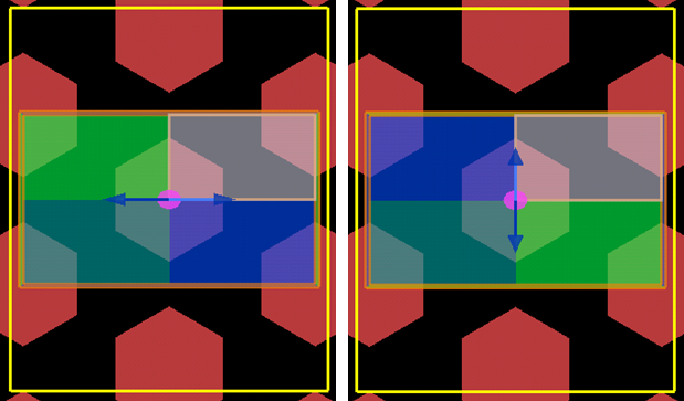
Open the solar_silicon_pillar.fsp project file. For this example, the FDTD solver is configured with the lowest accuracy mesh settings to reduce the simulation time. Note that the boundary conditions for the FDTD solver (symmetric/anti-symmetric) and the source polarization angle are set by model setup script based on the polarization property (0 or 1). The pillar structures are generated by the "pillars" construction group, where the diameter, pitch, height, and other properties can be adjusted.
The "solar_generation" analysis group is used to calculate the generation rate of electron-hole pairs in silicon for exporting to the electrical simulation in CHARGE. In the analysis group, the export filename property is specified by the model setup script, and is adjusted based on the polarization of the plane wave source. The data files will be named silicon_pillar_G_s and silicon_pillar_G_p for the two orthogonal polarizations. When the data is imported into CHARGE, the two orthogonal polarizations will be summed. Please note that since it uses 3D index and profile monitors, the memory requirement is high during simulation and longer simulation time should be expected. Due to strong variation of transmission spectrum, we use larger amount of frequency points (561) in "monitor".
In the optimizations and sweeps toolbox, a parameter sweep "pol" is included, which will run the two simulations for the orthogonal polarizations. Both the ideal short-circuit current and the transmission will be recorded. Before running the parameter sweep, use the simulation memory requirements check ![]() to verify that sufficient memory and storage is available for this simulation on your computer.
to verify that sufficient memory and storage is available for this simulation on your computer.
The top cladding of the structure is assumed to be air, with a refractive index of unity. Any native surface oxide is neglected. In the FDTD simulation, the silicon substrate is layered on top of an index-specified (1.4) material.
CHARGE simulation
The CHARGE simulation region is 3D as well. For the silicon pillars, import doping objects are used, and the surface-conforming doping profile has been generated from the solar_silicon_pillar_doping.lsf script according reference design parameters [Garnett10]. The doping profile is included in the project file using the doping import objects. You can run the provided script to re-generate all of the import doping data. Since the boundaries in CHARGE imply a symmetry, it is sufficient to simulate one quarter of the unit cell, which is equivalent to the FDTD simulation volume. The two optical generation rates, representing the orthogonal polarizations, are imported from the FDTD simulation. The optical generation rates are automatically accumulated in CHARGE. Note, in CHARGE, a scale factor is needed in the Optical Generation Rate objects to scale the output result by 50% (required for averaging the two polarizations).
Optical simulation results
Open the solar_silicon_pillar.fsp project file and Run the parameter sweep "pol" in the "Optimzations and Sweeps" panel.
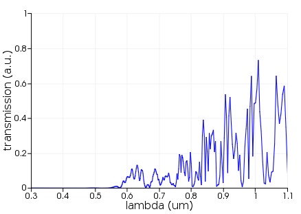
When the sweep is complete, the ideal short-circuit current and transmission spectra will be available in the "pol" sweep results. The sum of the ideal short-circuit current is about 64 mA/cm2 (recall that each generation rate will be scaled by 0.5 in CHARGE), indicating that 70% of the available solar energy was absorbed in the thin-film. A plot of the transmission indicates that most of the light wavelengths shorter than 800nm are absorbed. Transmission is larger for the longer wavelengths than the referenced design, which is likely due to the high degree of symmetry in the simulated device (additional surface roughness and variation in pillar height in the actual solar cell would enhance light trapping through scattering) [Garnett10].
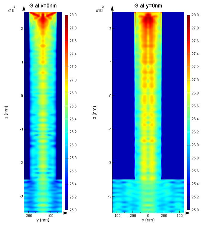
It is also possible to open the sweep files individually (the files are saved in the "solar_silicon_pillar_pol" sub-directory). The solar generation rate analysis can be re-run in each project file with the make plots property set to 1, which can be used to visualize the generation rates calculated in FDTD. These plots illustrate the light-trapping in the pillars, and the reduced absorption in the substrate.
Electrical simulation results
The CHARGE solver can be used to characterize the complete optoelectronic response of the solar cell. As described in the simulation setup, the structure and doping profile follow the reference design. In CHARGE, two modifications are made to the setup for simulation convenience. First, the top cladding volume (air in the FDTD simulation) is filled with SiO2: this enables the specification of surface interface properties that would be expected between the silicon and thin native oxide, but will not influence the electrostatics. Second, contacts are specified at the top (in contact with the tops of the pillars) and bottom (replacing the specified-index material). This choice maintains the symmetry within the unit cell, minimizing the simulation volume required.
Open solar_silicon_pillar.ldev project file. In the CHARGE solver region, the minimum and maximum edge lengths have been adjusted to give adequate resolution within the pillars, and the maximum number of refinement steps has been increased. Under the advanced settings, Fermi statistics are enabled to accurately account for the degenerate doping density in the conformal layer. In the doping group, note that two import objects have been used to specify the conformal (shell) doping for the pillars. As mentioned in the previous section, the doping profile is generated from the solar_silicon_pillar_doping.lsf script. A backside diffusion is also included to model the ohmic back contact - this is modeled with an analytic Gaussian distribution. The background silicon is assumed to be moderately p-type.
Two optical generation rate imports are also included in the layout. These represent the two orthogonal polarizations from the FDTD simulation, and include the imported data from those calculations. The optical generation rate objects are applied cumulatively to the semiconductor regions in CHARGE, such that the averaging of the two polarizations (which needs 50% scaling here) is done automatically in CHARGE.
As with the FDTD project, the pillars are added to the layout using a construction group. In the CHARGE project, top (emitter) and back (base) contacts have also been added to the layout. These objects are associated with two ohmic contact models, which can be found in the Boundary Conditions table. The base contact is specified with a sweep over voltage values ranging from 0 to 0.53V. Additional voltage points are included near the open-circuit voltage to better resolve the IV curve in this range. In the contact model for the base, both series and shunt resistances are included. Rsh and Rse are equivalent to the resistance values for a 1cm2 device, and are normalized by the surface area of the solver region (analogous to having many unit cells connected in parallel).
Run the simulation. When the simulation is complete, open and run the script file solar_silicon_pillar_plot_JV.lsf to generate plots of J and P vs. V (c.f. Fig. 3a of Garnett10). In the plot below, the data extracted from the reference is shown for comparison.
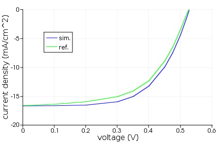
To obtain this agreement between results, the carrier lifetimes in silicon were adjusted to match the short circuit current density and diode ideality. A series resistance (for the 1cm2 cell) was specified at 1Ω, and the shunt resistance was then adjusted to match the open circuit voltage. A comparison of results is summarized below.
|
JSC (mA/cm2) |
VOC (V) |
η (%) |
|
|---|---|---|---|
|
CHARGE |
16.8 |
0.52 |
5.8 |
|
Ref. [Garnett10] |
16.5 |
0.525 |
4.8 |
Reference
Garnett, E. & Yang, P. Light Trapping in Silicon Nanowire Solar Cells. Nano Lett. 10, 1082–1087 (2010).