This example describes the simulation of a npn bipolar junction transistor (BJT). In the first part we will perform steady-state simulations to calculate the current-voltage characteristics and the current gain of the BJT. In the second part of this example we will perform a small-signal analysis to calculate the unity-current-gain cutoff frequency (fT) of the transistor.
A project file is provided to assist with the application example. The project file contains the material properties, geometry, and simulation region required to run the example.
Simulation setup
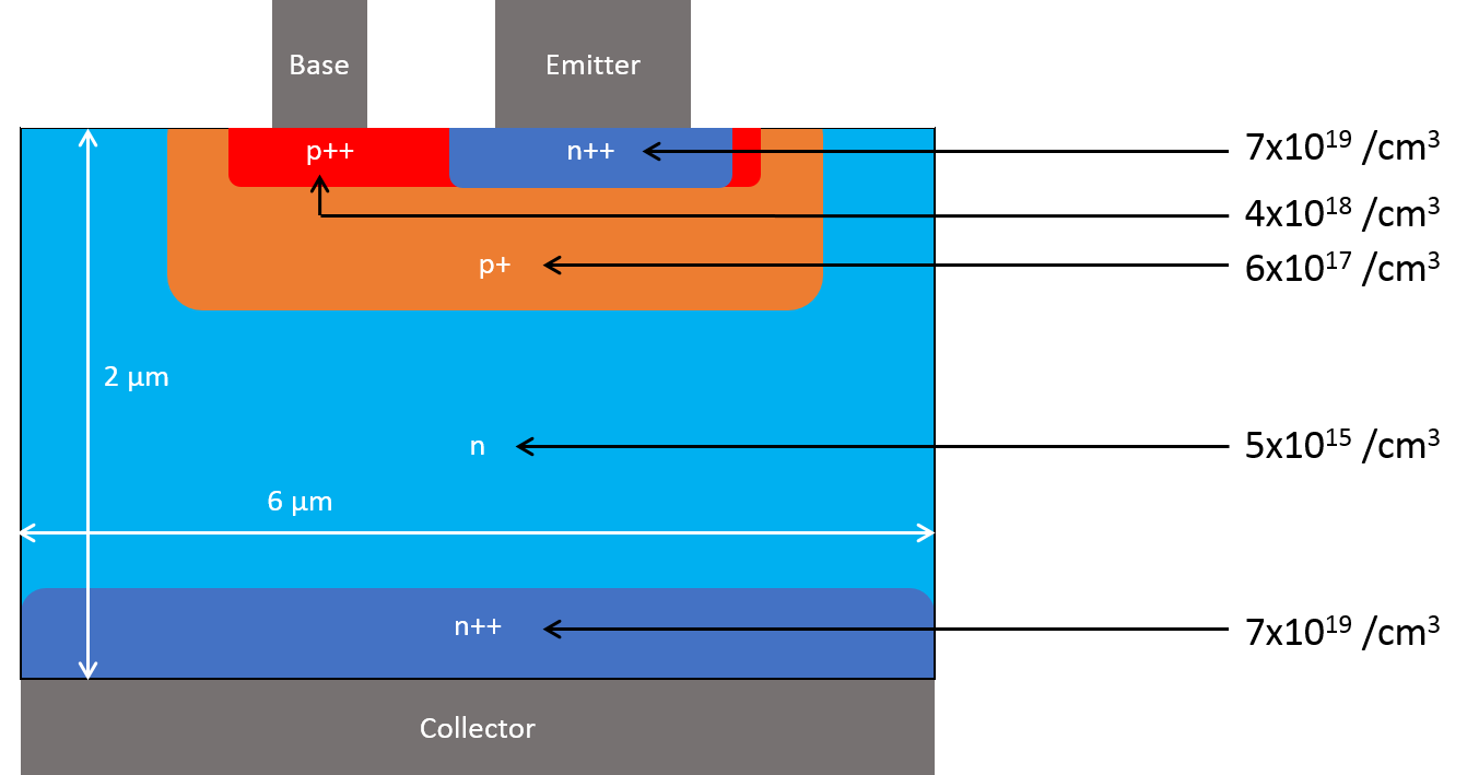
Download the npn_BJT.ldev and npn_BJT_ini.ldev project files and save them in the same folder. Open the npn_BJT_ini.ldev project file in CHARGE. The file already contains the geometry of the BJT, the doping profile, boundary conditions, and the CHARGE solver region. The schematic of the npn BJT can be seen in the figure below. There are two back-to-back pn junctions between the emitter and the collector contacts. The common p region between the two n regions is connected to the third contact, base. Due of the back-to-back pn junctions, there is no conduction path between the emitter and the collector. However, if the base-emitter junction is set into forward bias mode by applying a positive voltage in the base contact, majority carriers (electrons) from the emitter entering the base (now minority carriers) get swept into the collector region under the electric field in the space charge region (of the base-collector pn junction) and conduction occurs between the collector-emitter junctions.
Run and results
Run the npn_BJT_ini.ldev project file. The boundary conditions are set up to sweep the collector voltage from 0 to 3 Volts while keeping the base and emitter contacts grounded (V = 0 V).
Doping profile
Once the simulation finishes running, right click on the solver region and visualize the "doping" dataset. The visualizer window will open and the doping profile of the BJT will be plotted. To get the plot shown below, select the "N" attribute in the doping dataset and plot the "Abs" value. Next from the property editor of the visualizer, choose to plot in log scale.

Steady-state analysis
Save the file with the simulation results and open the npn_BJT_steady_state.ldev project file. Go to the properties of the "CHARGE" solver region and ensure that the "Continue from Previous Solution" option is enabled and that the npn_BJT_ini.ldev project file has been selected. This will allow the solver to load the results from the previous simulation (collector voltage at 3 V) and use it as an initial guess. The boundary conditions have been set up to keep the collector voltage at 3 V and the emitter voltage at 0 V (ground). A voltage sweep has been applied to the base contact to sweep the voltage from 0.2 V to 0.9 V in 8 steps. Run the simulation and use the npn_bjt_get_plots.lsf script file to plot the base/collector currents vs base voltage and beta vs collector current results:


The base current behaves similar to that of a forward biased pn junction with an exponential growth with applied bias (linear in log scale). The collector current starts at extremely small value at small base voltage when the BJT is turned off. As the base emitter junction enters forward bias, the BJT turns on and the collector current picks up until it reaches saturation. This can be seen from the base to collector current amplification factor (beta) plot on the right.
Small signal analysis
The large base to collector current amplification factor (beta) of BJTs make them suitable for building amplifiers. By applying a suitable DC bias the keep the BJT in active region, the transistor can be used to amplify small-signal ac inputs. The small-signal behavior of the BJT can be simulated using the small-signal ac (ssac) solver in CHARGE. To do this, download and open the npn_BJT_ac.ldev project file.
The file has been set up to sweep the base voltage from 0.2 V to 0.9 V and perform small signal analysis at each bias point. Once the simulation is run, the solver calculates the small signal voltages and current at different terminals. Run the simulation and use the npn_bjt_plot_fT.lsf script file to plot the results. The following plot shows the small-signal current gain of the BJT at a base voltage of 0.8 V as a function of frequency in log scale. At low to moderate frequency of operations, the BJT provides a constant current gain. At high frequency however the gain rolls off and eventually becomes smaller than 1.
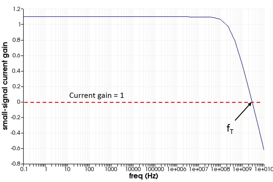
The frequency at which the small-signal current gain equals 1 is called the unit-current-gain cutoff frequency (fT) and is a widely accepted figure of merit to denote the bandwidth of a transistor. The plot below shows the fT of the BJT as a function of collector current.
