This example shows how to simulate an elecro-optical modulator based on the shown graphene waveguide. The chemical potential of graphene can be tuned by applying an external biasing voltage, this provides a mechanism to modulate the propagation losses of the waveguide.
graphene_electro_optic_modulator.lms
Optical simulation
Simulation setup
The project file graphene_electro-optic_modulator.lms sets up a 2D FDE simulation based on a cross section of the waveguide as well as a 3D EME simulation based on a 40μm long waveguide. Note that two layers of graphene - one on top and another one on the side - partially cover the waveguide core. The graphene material type described in Modeling methodology is used to model the two graphene layers following the surface conductivity approach. In both cases, a scattering rate of 15meV and a temperature of 300K are employed. As a first step, the modulator is simulated in both the minimum and maximum absorption states. To model these two states, two different sets of chemical potentials are employed:
|
Chemical potential for |
minimum absorption |
maximum absorption |
|---|---|---|
|
top sheet |
0.516eV |
0.0930eV |
|
side sheet |
0.560eV |
0.0103eV |
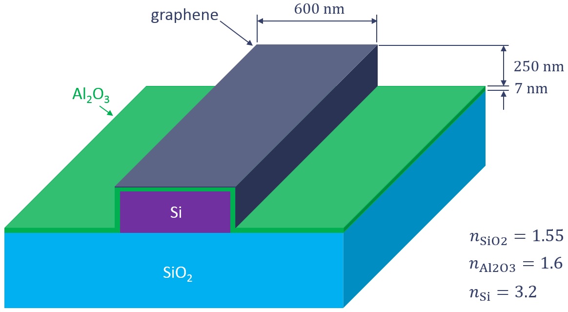
The modulator is meant to operate using the waveguide mode shown below. The plot was generated using the 2D FDE simulation set up in graphene_electro-optic_modulator.lms. The effective index of the mode is 1.78 for a wavelength of operation of 1.53μm. The cross-sectional field profile of the mode does not change significantly for the minimum and maximum absorption states, however, the losses can change dramatically as explained next.
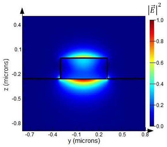
In the minimum and maximum absorption states, the 2D FDE simulation predicts losses of 0.0112dB/μm and 0.117dB/μm, respectively, which are close to the values quoted in the referenced paper. The 3D field distribution along the propagation direction (x axis) can be generated for both the minimum and maximum absorption states by activating the 3D EME simulation set up in graphene_electro-optic_modulator.lms. The resulting electric field amplitude along the propagation direction in both the minimum and maximum absorption states is shown below.

E-field amplitude along the propagation direction: minimum absorption (top) and maximum absorption (bottom) states.
To improve the calculated loss, it is necessary to employ a more realistic model of the refractive index in the silicon core. To this end, the project file graphene_electro-optic_modulator.lms contains electron-hole density material attributes that were imported from CHARGE. The script graphene_electro-optic_modulator_transmission_calc.lsf sweeps the biasing voltage of the modulator and activates the appropriate electron-hole density material attributes depending on whether a positive or a negative biasing voltage is used. To know what chemical potential corresponds to a given biasing voltage, a mapping was generated in the CHARGE and exported to two text files: mu_vs_voltage_top.txt and mu_vs_voltage_leftwall.txt. These text files are loaded by the script and used to map any given biasing voltage to a chemical potential. The CHARGE simulation uses an approximate volumetric model to simulate the electrical properties of graphene surface. The model has been tested against analytic results and the details can be found in the Electrical simulation section.
Results
When the script graphene_electro-optic_modulator_transmission_calc.lsf is run, it collects the losses for each biasing voltage and generates a plot comparing the computed results against the experimental values published in the referenced paper. The generated plot is shown in below. The experimental values are stored the text file graphene_electro-optic_modulator_paper_data.txt.
![]()
Electrical simulation
The graphene-based electro-optic modulator under investigation achieves modulation by tuning the Fermi level of the graphene layers. A gate voltage is applied to the graphene sheet that shifts the Fermi level of the material and modifies its optical absorption rate. The modulation in the optical absorption rate of graphene modulates the optical response of the silicon waveguide. Investigating the complete electro-optical response of the modulator requires a combination of electrical and optical simulations. In this section, we discuss the electrical simulation of the modulator using the CHARGE solver.

Modulation in graphene's optical absorption with applied bias voltage
CHARGE employs an industry standard drift-diffusion solver capable of handling complex geometries. The semi-classical solver in CHARGE uses an effective-mass, 3D density-of-states (DOS) to model semiconductor materials. This poses a challenge when it comes to modeling the 2D DOS of graphene. By using the electron (and hole) effective mass, me (and mh) and bandgap (or conduction band minima, Ec) as fitting parameters, we can tailor the 3D DOS used by CHARGE to mimic the 2D DOS of graphene. The resulting model, while not physically accurate, is able to calculate the carrier density of graphene with reasonable accuracy and can be used as a good first approximation.
Electrical model for graphene in CHARGE
The 2D DOS of graphene can be described by the analytical equation,
$$ g(E) = \frac{2|E|}{\pi \hbar^2 \nu_F^2} $$
where, vF = 106 m/sec, is the Fermi velocity in graphene and E is the electron energy. On the other hand, the 3D DOS of a conventional semiconductor has the following form,
$$g(E) = \frac{\sqrt{2}}{\pi^2} \left( \frac{m^*}{\hbar^2}\right)^{3/2} \sqrt{E - E_c}$$
where, m* is the electron (or hole) effective mass, E is the electron energy, and Ec is the energy at the bottom of the conduction band.
In a semi-classical model, the DOS, g(E) can be used to calculate the carrier density of a semiconductor. For the zero-bandgap graphene, the 2D electron density (/cm2) can be calculated as,
$$ n_{2D} = \int^\infty_0 g(E)f(E)dE = N_{c, 2d} \int^\infty_0 \frac{E}{1 + \mathrm{exp}((E - E_F)/(kT))} dE$$
Applying \(\varepsilon = E/(kT)\),
$$ n_{2D} = N'_{c, 2d} \int^\infty_0 \frac{\varepsilon}{1 + \mathrm{exp}(\varepsilon - \eta)} d\varepsilon = N'_{c, 2d} F_1(\eta)$$
where, \(N'_{c, 2d} = \frac{2(kT)^2}{\pi \hbar^2 \nu_F^2}\) is the 2D effective DOS, EF is the Fermi level, k is the Boltzmann constant, T is the temperature, and F1 (η) is the Fermi-Dirac integral of order 1 with η=EF⁄kT.
The 3D DOS can be used in a similar manner to calculate the 3D electron density (/cm3) of a semiconductor giving,
$$ n_{3D} = N'_{c, 3d} \int^\infty_0 \frac{\sqrt{\varepsilon}}{1 + \mathrm{exp}(\varepsilon - \eta)} d\varepsilon = N'_{c, 3d} F_{1/2}(\eta)$$
where, F1⁄2 (η) is the Fermi-Dirac integral of order 1/2 with η=(EF-Ec)/kT, EF is the Fermi level, Ec is the energy at the bottom of the conduction band, \(N'_{c, 3d} = \frac{1}{\sqrt{2}}\left(\frac{m^* kT}{\pi \hbar^2}\right)^{3/2}\) is the 3D effective DOS, and m* is the electron effective mass.
It is a matter of using a simple scaling factor to resolve the mismatch between N'c,2d and N'c,3d. Using m* and Ec as fitting parameters along with this scaling factor, we can compare the electron density of graphene calculated by the 3D DOS used in CHARGE with the actual electron density calculated by the 2D DOS. The figure below shows that using m*=1.768, and Ec=0.1 eV, the electron density (/m2) of a 1 nm thick (3D) graphene sheet in CHARGE is in good agreement with the analytic electron density of 2D graphene.

By comparing the electron density from the CHARGE model more carefully with the analytical electron density of 2D graphene, we have identified that the accuracy of the 3D model can be further improved by using different fitting parameters for different ranges of Fermi level. We have therefore created two material models for graphene in CHARGE; 'graphene_1 (Ef ≤ 0.05 eV)’ models the 2D electron density of graphene in a 0.1 nm thick 3D graphene sheet when the Fermi level is near or below Dirac point (Ef ≤ 0.05 eV), and ‘graphene_2 (Ef > 0.05 eV)' models the 2D electron density of graphene in a 0.75 nm thick 3D graphene sheet when the Fermi level is well above Dirac point (Ef > 0.05 eV).
3D equivalent electrical models of graphene in CHARGE
|
Model |
graphene_1 (Ef ≤ 0.05 eV) |
graphene_2 (Ef > 0.05 eV) |
|---|---|---|
|
Range of EF (eV) |
≤ 0.05 |
0.05 |
|
m* |
1.768 |
0.4614 |
|
Ec (eV) |
0.1 |
0.1 |
|
Thickness of graphene sheet (nm) |
0.1 |
0.75 |
Electrical simulation Setup
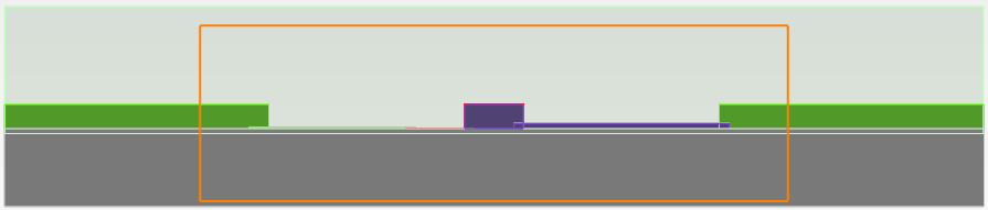
The above figure shows the cross-section of the simulation setup in CHARGE on the YZ plane.The attached CHARGE files graphene_electro-optic_modulator_1.ldev and graphene_electro-optic_modulator_2.ldev contains the modulator geometry which is identical to the setup in the optical solver. The two files use two different models for graphene to simulate the device in the appropriate bias ranges. The silicon waveguide is shallow doped with an acceptor concentration of 1018 /cm3. Two bandstructure monitors ‘band_top’ and ‘band_leftwall’ record the Fermi levels of the graphene layers on top and on the left wall. The charge monitor ‘charge_wg’ records the charge variation in the silicon waveguide with respect to gate voltage.
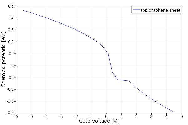
Once the simulation is run on both CHARGE files, the script files get_top_Ef_data.lsf and get_leftwall_Ef_data.lsf can be used to read the variation in the chemical potentials of the graphene sheets on top and on the left wall. The chemical potential of the top graphene sheet as a function of the gate voltage is shown below. The CHARGE files also save the charge profile of the silicon waveguide as a function of gate bias in two Matlab data files charge_wg_graphene_1.mat and charge_wg_graphene_2.mat which can be incorporated in the optical simulation.
Related publication
- M. Liu et. al., "A graphene-based broadband optical modulator," Nature Lett. Vol. 474, 64-67 (2011).