
In this example, we will calculate the optical spatial generation rate from a 3D device using FDTD for later use in an electrical simulation using CHARGE.
Optical simulation
Simulation setup
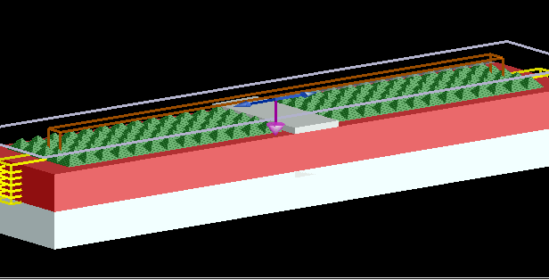
The structure in this simulation is a 3um thin film of silicon with TiO2 patterning on the upper surface, on a glass substrate. The TiO2 patterning is designed to enhance the device performance in several ways, including:
- Enhance optical efficiency by acting like an AR coating. It is expected to reduce reflections and increase the fraction of power absorbed in the silicon active layer.
- Maintain efficient electrical characteristics by minimizing the silicon surface area. Reducing the silicon surface area is expected to minimizes electrical surface recombination effects that lowered the efficiency of the 2D silicon grating solar cell described in the previous example.
Also, a large metal contact appears every 24 periods to collect the generated current. We usually ignore this contact in the FDTD simulation, so the simulation volume can be restricted to a single unit cell. The contact will be included in the CHARGE simulation.
The setup for this example follows the guidelines described in Typical simulation setup in FDTD. We use a plane wave source with bandwidth 400-1100nm, which covers the majority of the solar spectrum. Typically, two simulations would be required to obtain the response of the system to unpolarized sun-light, as described in the 3D pillar silicon solar cell example. However, due to the symmetry of this structure, a single simulation is sufficient, although some care is required to calculate the unpolarized response correctly.
Generation rate measurement: We use the solar_generation analysis object, available in the Object Library, to measure the spatial generation rate. For meshing purpose in CHARGE, we intentionally set the size of generation object slightly larger then the silicon in z direction.
|
Warning: Large memory requirements The generation rate analysis object collects electric field and material data as a function of position (3D) and frequency. This 4D data-set can result in very large data files when the simulation volume is large, when the mesh is small, or when you collect a large number of frequency points. Also, post-processing, when the analysis script calculates the generation rate from the raw monitor data, requires additional memory (RAM). We strongly recommend using the spatial downsampling option and minimizing the number of frequency point to reduce the memory requirements, at least for your initial simulations. |
Results
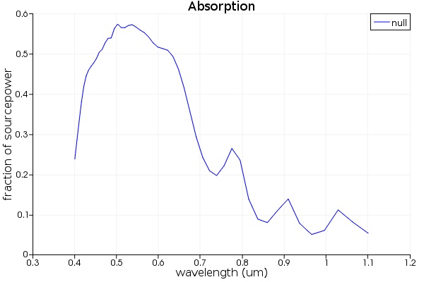
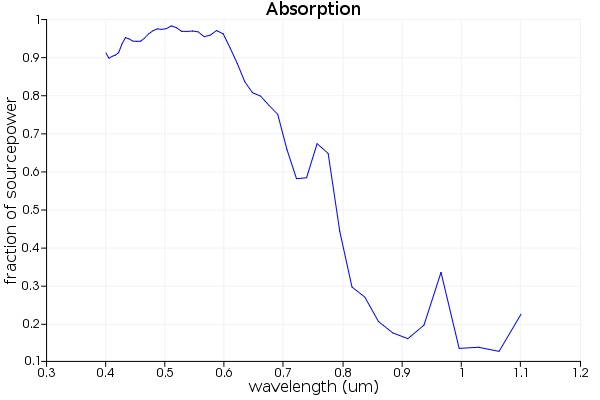
The following table summarizes a number of the most interesting simulation results. For reference, we compare the simulation results to a silicon slab without the TiO2 patterning.
|
Quantity |
no patterning |
TiO2 pyramids |
|---|---|---|
|
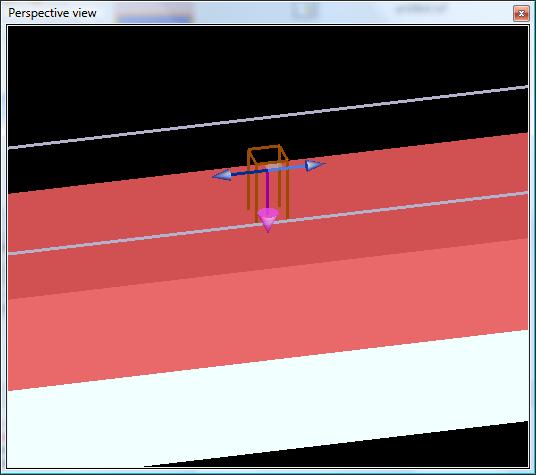
Screenshot of simulation |
|
|
|
Fraction of source power absorbed in silicon region. Note: This result is not re-normalized to the solar spectrum. |
|
|
|
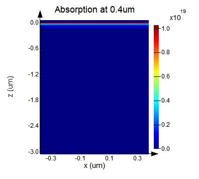
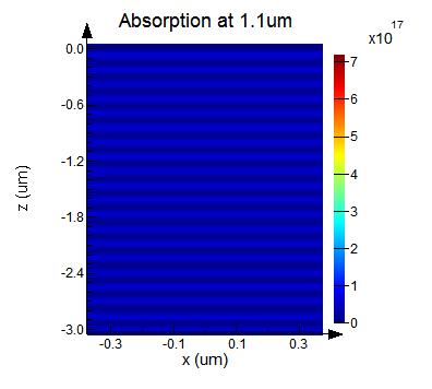
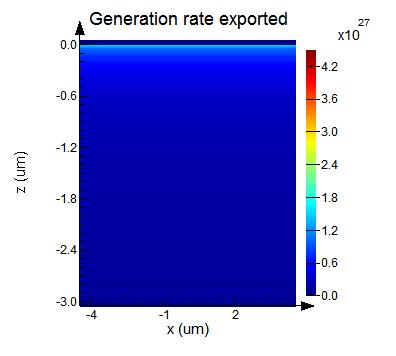
Spatial absorption profile at 400nm Due to the high absorption of silicon at 400nm, the absorption is concentrated near the silicon surface |
|
note: scale is 1e27 |
|
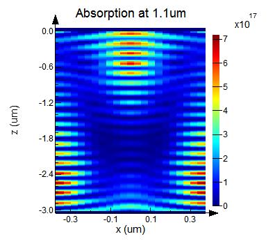
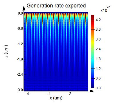
Spatial absorption profile at 1100nm At 1100nm, silicon absorption is much lower, leading to absorption throughout the silicon layer. We also see an interference pattern due to reflections at the interfaces. |
|
|
|
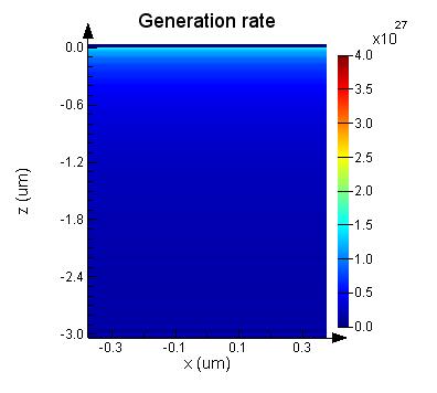
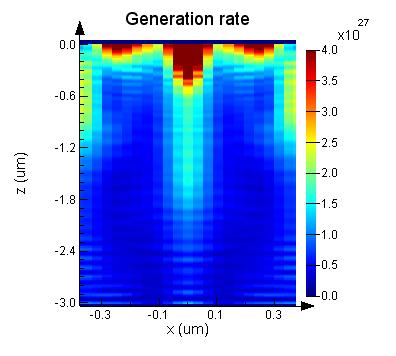
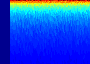
Generation rate profile The generation rate data is obtained by normalizing the absorption data to the solar power spectrum, then integrating over all wavelengths. |
|
|
|
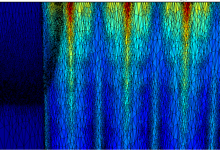
Generation rate profile to export The generation rate object provides some additional options that can be applied to the generation rate data before it is exported to CHARGE. In this screenshot, the data has been averaged in the Y dimension, and arrayed 3 times. |
|
|
|
Short circuit current |
120 A/m^2 |
250 A/m^2 |

|
Note: To reproduce the results shown above, run the simulation, then use solar_pyramid.lsf. To reproduce the unpatterned results, disable the pyramid object from the simulation file. For 2D CHARGE simulation, export the generation data from "solar_generation" analysis group by modifying "average dimension" to be "y". For 3D CHARGE simulation, simply change the "average dimension" to be "none", and rename the export file name. |
2D electrical simulation
CHARGE can be used to more completely characterize the electrical characteristics of the solar cell, as described in the previous pages. As a beginner's example, we can simplify CHARGE simulation in 2D. Two common approaches are shown in the following figure.

Average over 3rd dimension
In many cases, the electrical aspects of a system are essentially 2D, even if the optical aspects are 3D. In such cases, averaging the generation rate over the 3rd dimension can be a very good approximation.
The TiO2 pyramid structure described on this page is an example of a structure where the averaging technique is appropriate. The TiO2 pyramids obviously give the system a 3D geometry. However, if we carefully consider the system from an electrical perspective, it becomes clear that the structure is effectively a 1D (TiO2 - Si - Air). The thickness of the TiO2 is not relevant because it is an insulator (not electrically active).
Slicing
An alternate approach is to run a series of CHARGE simulations, where each simulation uses one slice of the generation rate data. This approach requires more CHARGE simulations, but it may provide more correct results for structures with some electrical structure in the 3rd dimension.
Short circuit current
When the FDTD simulations are complete, the generation rate data can be imported into CHARGE solver with the 'Import Source object. The following script can be used to output the short circuit current.
Jsc=getdata("CHARGE","emitter.I")/(getnamed('CHARGE','norm length')*getnamed("CHARGE simulation region","x span"));
?"Short circuit current: "+num2str(pinch(Jsc))+" A/m^2";
As expected the short circuit current is slightly (~200) lower than the value from FDTD (~250). This is partly due to the shadowing by the emitter contact and partly due to recombination effects, both of which are not included in the FDTD simulation.
Additional simulation results can be plotted with the results visualizer, such as viewing the mesh and imported generation rate profiles. An obvious next step is a voltage sweep, which would allow you to calculate the solar cell efficiency, as shown in the previous example.
|
Quantity |
no patterning |
TiO2 pyramids |
|---|---|---|
|
Short circuit current |
120 |
200 |
|
Meshed generation rate profile (imported from FDTD) |
|
|
|
Advanced note: Including the contact shadowing in your FDTD simulation The above FDTD simulation used periodic type boundary conditions to simulate a perfectly periodic array of pyramids. It did not include any effects from the metal contacts that are required to collect the current generated within the solar cell. This approximation makes the FDTD simulation much faster, as we only need to simulate a single unit cell. To check the validity of this assumption, we can run an FDTD simulation that includes the contact. The following commands can be used to adjust the simulation setup to include the metal contact and 12 periods of the pyramid patterning. Remember that the memory requirements will be greatly increased. You may also need to make some further modifications, such as using several small generation rate monitors, rather than one large generation rate monitor, as several small monitors make the generation rate calculation more memory efficient. You should check the memory requirement before running it! # full structure
setnamed("Skewed rectangular pyramid1","x",1.5e-6);
setnamed("Skewed rectangular pyramid2","x",-10.5e-6);
setnamed("emitter","x",0);
setnamed("base","x",0);
setnamed("FDTD","x span",20.25e-6);
setnamed("solar_generation","export filename","pyramid_full");
setnamed("solar_generation","periods",1);
save("pyramid_full");
|
After running the simulation, the generation rate data from this simulation can be imported into the CHARGE file provided above. The short circuit current, Jsc from CHARGE with this new 'full' generation rate data from the large FDTD simulation is about 196 A/m^2. This is very similar to the 200 A/m^2 found in the original simulation, which shows that the assumption to ignore the metal contact in the FDTD simulation is reasonable.
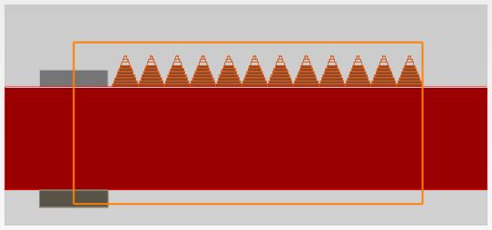
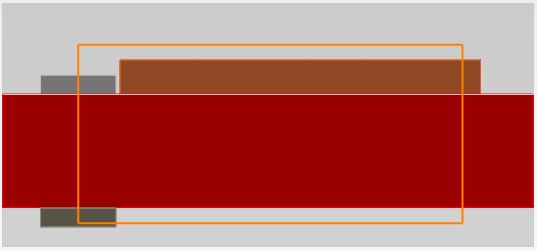
It is interesting to note that, although the pyramid is critical for optical simulation, its shape has little effect on the electrical simulation! This is because the pyramid material TiO2 is optical dielectric but electrical insulator, so the carries do not interact with insulator. This can greatly simplify the meshing and simulation, since we can use a slab TiO2 to replace the pyramids, the latter needs much more elements. In the solar_pyramid_2D.ldev, you can disable the pyramid objects and enable the "TiO2" object, which will give you almost identical result. This can help us simulate the 3D case easily.
3D electrical simulation
In the previous section, we discussed how the 3D solar cell can be modeled in 3D in FDTD but averaged over the third dimension and exported into the 2D CHARGE CAD. 2D simulations are faster than 3D simulations, however, 3D simulation of a structure will ensure accuracy of the results. It is also useful for 2D structures where averaging may not be feasible. We will see that for this particular structure because of the symmetry of the device, 2D and 3D results will be in close agreement.

The optical simulation in 3D is about the same as the 2D case, except that the exported generation data is not averaged in any direction, and it is output automatically once you run the analysis. Once the file of generation data is ready, you can import it into CHARGE for electrical simulation.
The simulation setup for CHARGE is in 3 dimensions. One full period in the third dimension is simulated. To keep consistent with the referenced paper and the 2D example, we simulate 12 periods in the x direction. We can just use the 3D import generation object in the CHARGE CAD and run the simulation. The solver type is now 3D . As tested in the solar_pyramid_2D.ldev 2D case, we will use a TiO2 slab instead of the original periodic pyramids to reduce the memory requirement.
using pyramid structure
using a TiO2 slab
When the FDTD simulations are complete, the generation rate data can be imported into CHARGE simulation file with the 'Import Generation' object by choosing "average axis" to be "none". A screenshots of the 3D simulation set up are shown above.
After running the simulation without applying voltage, the following command can be used to output the short circuit current.
area = getnamed("CHARGE simulation region","x span")*getnamed("CHARGE simulation region","y span");
Jsc=getdata("CHARGE","emitter.I")/area;
?"Short circuit current: "+num2str(pinch(Jsc))+" A/m^2";
As expected and as in the 2D case the short circuit current is lower (~199 A/m^2) than the value from FDTD (~245). This is partly due to the shadowing by the emitter contact and partly due to recombination effects, both of which are not included in the FDTD simulation. Note that the 2D and 3D electrical simulation results are in agreement. The 3D results are obviously more accurate; however, in this particular case, due to the symmetry of the charge distribution in the third dimension,the 2 dimensional simulation electrical simulation provides a sufficiently accurate approximation for full device characterization.This is one example that people can just simulate 2D to get a quick and reasonably result.
We can go further by sweeping the bias and observing the current-voltage characteristics of the device. Lock the mesh to avoid having to mesh the simulation again. Then, switch back to the layout mode and click the edit button for base bias value to modify it. Check the DC box and set the voltage to rage from 0 to 0.7 Volts in 15 steps (from the results below, you can simulate 0.6 v in 13 steps to save simulation time). Then run the simulation again. and use solar_plot_J_V_Power.lsf to plot the results.

Applied voltage vs. Current density

Applied voltage vs. power density
Efficiency values (~9.3%) can be extracted from this plot by dividing the maximum power by the input power of 100 mW/cm2The open circuit voltage for the solar cell can also be extracted from the x crossing of the plot.
Reference
Teck Kong Chong, Jonathan Wilson, Sudha Mokkapati and Kylie R Catchpole, "Optimal wavelength scale diffraction gratings for light trapping in solar cells," J. Opt. 14 (2012) 024012 (9pp) http://iopscience.iop.org/2040-8986/14/2/024012