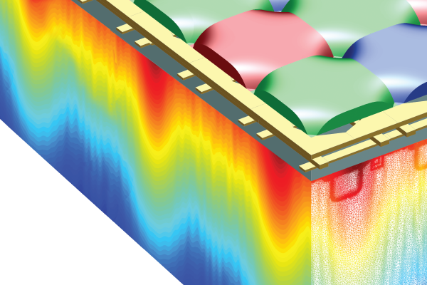
 As CMOS image sensor pixels sizes shrink to pixel diameters of 1 micron and below, there has been continued research into overcoming technical challenges related to the production of images of sufficient quality, color depth and resolution sufficient for demanding consumer and commercial applications. With the goal of producing CMOS imagers capable of capturing an incident light signal, and efficiently propagating that signal through sophisticated multilayer structures manufactured with CMOS fabrication processes, rigorous optical and electrical simulations that account for absorption, scattering, and diffraction from sub-wavelength features (like metallic interconnects for the readout electronics, or the curved dielectric surfaces of which the microlens array is constructed) as well as steady state and transient electrical behavior of the sensor are required.