In this example, we will study the performance of a lateral germanium-on-silicon photodetector with FDTD (optical simulation) and CHARGE (electrical simulation). Sensitivity of the responsivity to variations in the design parameters is analyzed.
Background
Photo-detectors convert optical signals into electrical signals to recover the information encoded on the optical channel. These components can be accurately simulated and optimized using a combination of optical and electrical solvers. The optical properties of the photodetector are simulated using the finite-difference time-domain (FDTD) method; the local generation rate of electron-hole pairs can be calculated from optical absorbed power. This generation rate then appears as a source term in the continuity equations solved in the electrical simulation (more information).
Typically, germanium is used as the absorbing medium in detectors for silicon photonics applications given its good absorbance in the C-band and its ease of integration into standard silicon CMOS processing [Guoiliang2012-Tseng2013]. In this application example, we present a simulation methodology for the sensitivity analysis and design optimization of a Ge-on-Si photodetector. This simulation methodology can be applied to typical detector layouts, including butt- and evanescent-coupled components, with active regions defined by lateral or vertical PIN diodes or in an MSM configuration.
Optical Design
Various configurations have been proposed for reducing the footprint and capacitance of the photodetector without sacrificing its responsivity [Michael2010]; simulations can be used to optimize these configurations and analyze the sensitivity to process-induced variations. To demonstrate the simulation methodology, we chose the device and enhancements proposed in [Guoiliang2012] as a reference design, which includes the addition of a distributed Bragg reflector (DBR) and point contacts that minimize absorption from the metal (see Figure 1a). In the 3D optical simulation with FDTD, the absorption coefficient used for germanium was 5 times larger than typical values for bulk germanium. This accounts for the increase in absorption for high-temperature-growth Ge films compared to bulk Ge [Guoiliang2012].

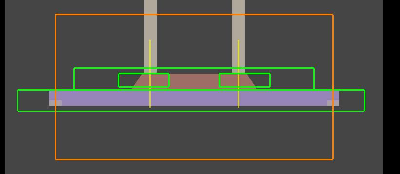
Open the project file lpd_sige.fsp. The model is parameterized so that multiple configurations can be generated by adjusting the properties of the model group at the root of the Objects Tree. Four different configurations can be simulated using the parameter sweep "configurations." This sweep is set up to adjust the properties enable_dbr and num_fingers described in the table below.
| enabled_dbr | num_fingers | configuration |
|---|---|---|
|
0 |
-1 |
no DBR, no contacts |
|
0 |
0 |
no DBR, continuous contacts |
|
1 |
0 |
DBR enabled, continuous contacts |
|
1 |
6 |
DBR enabled, 6 finger (point) contacts |
The contact dimensions and pitch can be specified using the setup properties of the model group and the contacts group. The dimensions of the DBR grating can also be adjusted through the properties of the grating group. For each configuration, the export data file name in the generation rate analysis object will be updated. Run the parameter sweep "configurations". Four optical generation rate data files will be saved in the sweep folder. These will be used for the electrical simulation in the following section.
The calculation of the optical generation rate (OGR) yields an upper bound on the responsivity of the detector. Assuming that each photo-generated carrier is collected ideally, the total current from the volume can be found from the integration of the OGR over the volume, multiplied by the unit charge. The input power is specified as 0.5mW in the generation rate analysis object. The configurations parameter sweep reports the value "Jsc," which is the ideal photocurrent normalized to the surface area. To calculate the ideal responsivity,
Jsc = getsweepresult('configurations','Jsc');
Iph = Jsc.Jsc*getnamed('generation_rate','x span')
      *getnamed('generation_rate','y span');
?R = Iph/getnamed('generation_rate','source power'); # responsivity in A/W
The ideal responsivities from the FDTD simulation are listed in the table in the following section.
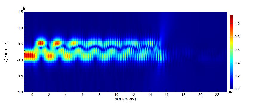
The electric field magnitude recorded in the cross-section along the centre of the photodetector is shown in the plot below (the following images are for the configuration with point contacts and a DBR). The E-field clearly shows an interference pattern in the Ge layer due to diffraction from the silicon waveguide and coupling between multiple modes. As suggested by [Guoiliang2012], contact absorption can be reduced by placing point electrodes in regions of minimal field intensity. Further, the design including the DBR can be optimized by choosing the length of the PD such that the maximum field is concentrated in the waveguide when it exits the PD, such that the majority of the un-absorbed radiation can enter the DBR and be reflected back to the PD for a second pass.
The power absorbed follows the electric field profile. It is plotted below for the cross-section along the length of the Ge volume.
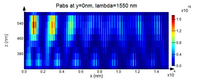
The generation rate is averaged along the length of the structure. This OGR is used as the input into the electrical simulation.

Electrical Design and Optoelectronic Response
Electrical simulations are performed in CHARGE on a 2D cross-section of the design. Open the lpd_sige.ldev project file. The PIN diode is defined by n-type and p-type implants in the germanium with peak dopant density 1018cm-3. The germanium is assumed to form an abrupt heterojunction with the underlying 20Ω-cm (5x1014cm-3) p-type silicon. All contacts are specified as ohmic. The SOI (silicon) layer is grounded through a 10kΩ resistor to model substrate leakage. Note that the layout of the silicon layer is modified from the optical simulation to accommodate the body contacts without influencing the electrostatic response. To review the material models, open the material database. Both the default silicon and germanium material models have been modified for this simulation. A surface recombination velocity of 1e7cm/s is specified for the silicon-germanium surface, corresponding to a high surface defect density. The base carrier lifetimes (trap-assisted recombination) have been reduced to 10ns and 1ns for germanium and silicon, respectively. These values are chosen to reflect the response of the reference design and simulate thin-film materials with larger impurity concentrations.
Four optical generation rate (OGR) objects are included in the simulation corresponding to the different combinations of contact location and DBR inclusion simulated with FDTD. Five configurations for the design can be chosen by adjusting the contact and dbr properties of the root model object in the Objects Tree according to the table below. By adjusting the values of the contact and dbr properties, the correct OGR object will be enabled.
| contact | dbr | configuration |
|---|---|---|
|
-1 |
-1 |
no illumination |
|
0 |
0 |
no contacts, no DBR |
|
1 |
0 |
continuous contacts, no DBR |
|
1 |
1 |
continuous contacts, w/ DBR |
|
2 |
1 |
point contacts, w/ DBR |
A representative plot of steady-state dark- and photo-current at T=300K is shown in the figure below. In reverse bias, leakage current into the silicon substrate dominates. The photo-current is simulated using the generation rate calculated in the FDTD simulations and was averaged in the direction of optical propagation. To run the simulations required to generate this figure, open lpd_sige_compare_illum.lsf. This script will generate a sweep over the first and last configurations, simulating the forward and reverse bias characteristics independently (this is done to improve the simulation efficiency). When complete, the script will collect the results.
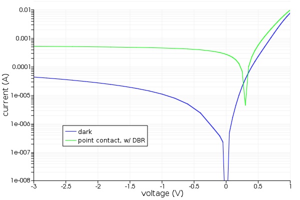
A comparison of responsivities for various configurations is listed in the following table, agreeing with the trend reported in [Guoiliang2012]. The input power is chosen to be 0.5mW, and the responsivity in CHARGE is calculated at a 0.5V reverse bias. The responsivity RFDTD is calculated assuming ideal collection of all photo-generated carriers.
| Contact | DBR | R_FDTD (A/W) | R_CHARGE (A/W) | R_CHARGE/R_FDTD (%) |
|---|---|---|---|---|
|
None |
No |
1.04 |
0.85 |
0.81 |
|
Continuous |
No |
0.91 |
0.73 |
0.85 |
|
Continuous |
Yes |
0.96 |
0.79 |
0.84 |
|
Point |
Yes |
1.12 |
0.90 |
0.84 |
Sensitivity Analysis
In the design of the reference device, the length of the Ge and point contact locations were chosen to optimize responsivity [Guoiliang2012]. Variation in the length of the fabricated structure and offsets to the contact locations may reduce the responsivity. To analyze the influence of these variations, a sequence of optical and electrical simulations are performed. One key design trade-off is the length of the PD vs. the responsivity. Open the lpd_sige.fsp project in FDTD. In this second of the application example, a parameter sweep that varies the length of the germanium structure will be performed. The configuration with the DBR enabled and point contacts will be simulated. Before beginning these simulations, change the number of point contacts to 5 (set the num_fingers property of the root model object to 5),
switchtolayout;
setnamed('::model','num_fingers',5);
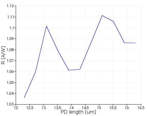
In a typical SiGe PD, the responsivity increases monotonically with the detector length as more light can be absorbed in the larger volume. With the inclusion of the DBR, the light is reflected and makes a second pass through the detector, so it is also important to optimize the amount of residual light from the first pass that is guided to the DBR. From the field profile plotted in the first section, the electric field intensity has a periodicity of approximately 2um. Therefore, we would expect to see enhancements of the responsivity when the length of the PD coincides with the maximum field intensity in the silicon layer (so that it will continue into the DBR).
In the optimizations and sweeps toolbox, edit the "pd_length" parameter sweep. The pd_length property is varied from 12.5um to 16.1um in 10 steps (0.4um increments). Run this parameter sweep.
| Note: As a large number of computationally intensive simulations are being run, it is useful to take advantage of all available computing resources. If available and supported by your licensing, the simulation time can be reduced by configuring your resources to take advantage of multiple workstations so that multiple simulations can be run concurrently. |
The following script can be used to plot the result
Jsc = getsweepresult('pd_length','Jsc');
lpd = getsweepresult('pd_length','pd_length');
Iph = Jsc.Jsc*lpd.null*getnamed('generation_rate','y span');
R = Iph/getnamed('generation_rate','source power'); # responsivity in A/W
plot(lpd.null*1e6,R,'length (um)','R (A/W)');
The figure below shows the responsivity as a function of PD length. As expected, the overall trend is the increase of responsivity with length, but clear peaks are visible where the optimal amount of light is directe&d into the silicon and DBR to be reflected for a second pass.
