In this example, FDTD is used to find the dispersion of a substrate integrated waveguide (SIW) and evaluate the leakage loss of its fundamental TE10 mode.
Background
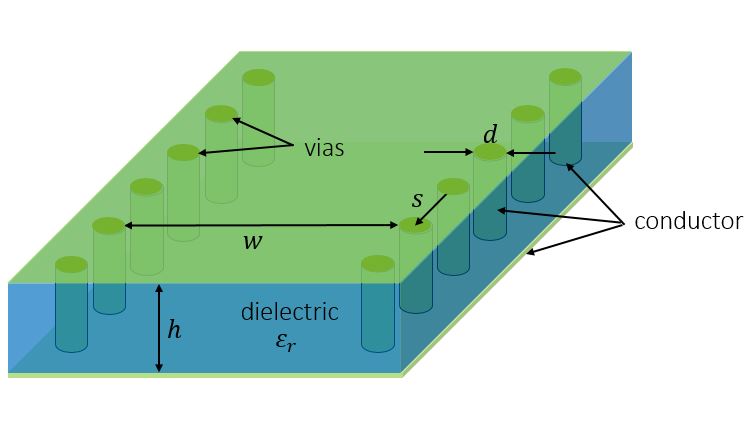
Shown in the above figure is the substrate integrated waveguide (SIW) which consists of a substrate loaded on its side-walls by a dense array of metallic vias that connect an upper and lower metal plates (Xu [1]). Similar to conventional rectangular waveguides, the SIW supports a spectrum of guided modes that propagate above their respective cutoff frequencies, the lowest being the fundamental TE10 mode. By using periodic vias in the SIW as opposed to the solid walls in the hollow waveguide, a small amount of energy is leaked outside of the SIW's interior. The amount of power leaked for an SIW waveguide is typically very small and can be characterized by the attenuation constant of the mode. In the absence of all other sources of loss (e.g., dielectric and ohmic loss), the attenuation constant accurately captures the loss due to this leakage.
Due to the periodicity of the side-via walls, the waveguide’s structure varies along the propagation direction and solving for the dispersion (or bandstructure) of the SIW can no longer be reduced to the 2D problem of the its cross section. For example, we were able to find the dispersion and cutoff frequencies of the coaxial and hollow waveguide through 2D simulations in MODE. For the SIW, a full 3D treatment in FDTD is required. The approach used here is similar to the photonic crystal waveguide (see the Waveguide PC bandstructure and Bandstructure a line defect waveguide (varFDTD) examples for details).
Simulation Setup
The simulation file substrate_integrated_wg.fsp contains the simulation model for this example and is shown in the figure above. The waveguide is composed of a rectangular substrate of height h=0.508mm possessing a relative permittivity εr=2.33 that is backed by 2D PEC conductor sheets on its bottom and top face. The substrate is loaded on its side by PEC via walls of radius d=0.7mm that are spaced s=2mm apart and separated by width w=7.2mm. Since the mode is largely confined between the via fences, the extent of the substrate outside them will have little effect on the mode’s dispersion. As such, we extend it out to an arbitrary width of 30mm.
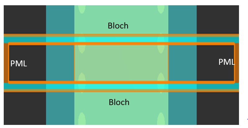
As this problem is interested in finding the bandstructure of the SIW, the simulation methodology provided in the bandstructure calculation methodology page is used extensively and will only be briefly reviewed here. The simulation regions z min and z max boundaries are assigned as metal and its x min and x max boundaries are assigned as PML regions. To speed of the simulation, only a single unit-cell is simulated with Bloch boundary conditions on the y min and y max boundaries and a propagation constant k defined between them.
The SIW is excited with the dipole cloud analysis group consisting of 10 randomly oriented and distributed dipoles placed between the via fences. In this example, only the TE10 mode will be evaluated and all higher-order modes are to be ignored. To ensure this occurs in the simulation, the bandwidth of the source must be properly set to cover only the TE10 monomodal bandwidth. Since the guided modes are forward-wave (i.e., phase increases with frequency) and the TE10 and TE20 modes’ cutoff frequency is near 14GHz and 29GHz, respectively, the bandwidth of the dipole sources is set to 8-23GHz. This is done through the global source properties.
|
Note : Location of dipole sources Setting the span of the dipole cloud such that dipole sources will be created outside of the waveguide’s interior could lead to the excitation of non-desired surface-type modes that are localized outside of the vias. Care should be taken to setup the region of the dipole cloud to be entirely inside the waveguide between the vias. |
The bandstructure calculation is carried out in the bandstructure analysis group. A sweep is used to calculate the resonant frequencies for each value of k, and construct the full bandstructure diagram. The leakage loss is found using the field_decay_slope analysis group. This analysis group calculates the slope of electric field decay for each value of k which is then used to find the leakage loss. A frequency monitor is used to observe the fields across a cross-section of the SIW halfway between adjacent vias.
|
Note : Finding a Mode's Attenuation Constant In order for the leakage loss calculation to be valid, only a single mode can be excited in the SIW. This is achieved by carefully limiting the bandwidth of the dipole sources and the range of k values to cover only the mode of interest. |
When obtaining the dispersion of modes using the bandstructure approach, the length of the simulation must be long enough to allow for the transients of the pulse to die away and the resonances of the SIW to be formed. A quick way to test this is to run the simulation for a fixed value of k and a large simulation length and observe the fields intensity versus time on any of the monitors.
Results and Analysis
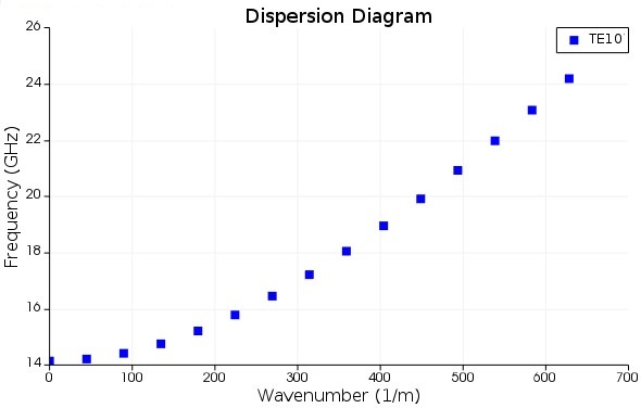
After opening up the FDTD file substrate_integrated_wg.fsp, the substrate_integrated_wg.lsf script is used to run the simulation and generate the results. After running the sweep with the set frequency limits for the source, the script extracts and plots the bandstructure for the band (after filtering out all unnecessary data points). The simulated results are plotted in the above figure. These results were obtained with a finer mesh setting in the SIWMesh with dx=dy=0.1mm.
The match between simulated and theoretical dispersion is clear. More accurate results can be obtained be increasing the frequency resolution and using a finer mesh over the vias. The script also generates a plot of electric field along the SIW’s cross section which shows the expected TE10 distribution.
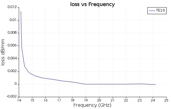
To calculate the leakage loss, the script calculates the group velocity from the slope of the TE10 mode’s bandstructure. This is then used with the log slope from the field_decay_slope analysis group to find the leakage loss in dB/mm which is shown in the above figure.
Related references
- Xu, Feng, and Ke Wu. "Guided-wave and leakage characteristics of substrate integrated waveguide." IEEE Transactions on microwave theory and techniques, vol. 53, pp. 66-73. (2005).