
When photonic crystals are used to make waveguides, the calculation of the photonic bandstructure becomes a 1 dimensional problem since the waveguide structure is only periodic in the direction of propagation. In this example we calculate the bandstructure and mode loss of the waveguide structure described in K. Ogawa et al.
Simulation setup
The waveguide has been drawn up in the simulation file waveguide3D.fsp, and is shown in the figure above. The waveguide is composed of a rectangular a Si3N4 rectangular core (1μm width and 400nm thickness), shown in green, on a 100 nm thick layer of Si with a triangular PC lattice of lattice constant a = 400 nm and hole diameter 260 nm. The holes are filled with SiO2 and the cladding above the waveguide core is also SiO2. The 100 nm thick Si layer is on a 1 μm thick layer of SiO2. The substrate is Si.
We use a different dipole cloud than the one in the Object library. The dipole cloud object that we use in this simualtion does not set the properties of the dipoles so that we are able to set them directly by modifying the global source properties. This allows us to easily create a narrowband source when we want to selectively excite the fundamental mode only.
Analysis
Before calculating the bandstructure, we will consider the type of results we expect. The waveguide is periodic in the direction of propagation, with period = a * sqrt(3), where a is the photonic crystal lattice constant. Since a = 400 nm, we have a period of approximately 693 nm. However, if we consider the microstructure along the direction of propagation of the waveguide, the 2D PC consists of alternating rows of holes, each row shifted laterally to the next. Apart from the lateral shift, there is no difference between the first row of holes and the second one. Therefore the structure is "nearly periodic" with a pitch of period/2. We can expect to see results that are nearly equivalent to a waveguide that is periodically modulated at a pitch of period/2=346.5nm. When the guide wavevector, k, equals 2π/period, there will be a barely observable bandgap. However, when the wavevector is 2π/(period/2) = 2*2π/period, we expect to see a large bandgap.
It should be noted, however, that the true period of the waveguide is 693 nm. Thus PC waveguide modes near the large "second order" band gap may have radiation components that contribute to loss. In addition, there may be some weak coupling at a wavelength of 1550nm to the Si substrate with the SiO2 cladding n=1.45 only 1 micron thick. Although this coupling mechanism is very weak, it will contribute to the loss over propagation distances of a large number of periods.
All modes
With the default settings in the simulation file, the sweep named Bandstructure will calculate the bandstructure for kx = 0-0.5. The script produces the plot below which includes points representing the zone-folded lightline for the cladding material (n=1.45). In the screenshot below, red lines have been drawn over the points composing the lightline for clarity. It should be noted that any modes above the lower branch of the lightline are lossy although the loss is very small, while any modes above the upper branch of the lightline are highly lossy. The waveguide bandgap is shown on the figure and the lower curve shows that the predicted gap is around f = 0.29. This corresponds to a wavelength range of approximately 1400nm. There is also a higher order mode supported in the waveguide at higher frequencies and it exists below the upper lightline. Some care might be required to avoid coupling light into this mode at the waveguide facet.

|
NOTE: for more accuracy, the waveguide bandstructure can be run again with twice as many grid points in x and y. This change will lengthen the amount of time required to calculate the bandstructure but will make the calculation of the bandgap more accurate. |
Fundamental mode
The bandstructure calculated above shows the waveguide has many modes. Here, we'll concentrate on the fundamental mode just below the gap at a normalized frequency of 0.27 (1500 nm, 200THz) for k=0-0.05.
Make the following changes to the simulation file:
|
Simulation region |
simulation time = 3000fs |
|
Global source settings We want a narrow source bandwidth to excite a few modes (ideally only one). This requires a longer time domain pulse and is the reason we increased the length of the simulation. |
frequency = 210 THz pulselength = 150 offset = 350 |
|
Model group |
In setup -> variables tab f1 = 200 THz f2 = 220 THz |
|
Parameter sweep |
kx end point = 0.05 number of points = 20 |
If you change the number of bands to 1 in the script file and re-run it with the updated parameter sweep mentioned above, the following plots will be created.

Dispersion and loss
With changes to the simulation described above, we are exciting a single mode of the device. In addition to calculating the bandstructure, it is also possible to calculate other properties of the mode, such as group velocity and loss. The script file automatically does these calculations when the bandstructure object returns data for only one band.
Loss
We can calculate the intrinsic loss of the photonic crystal waveguide. This is the loss due to the period of approximately 693 nm which allows weak coupling into the substrate.
The excitation and subsequent decay of the waveguide mode is sampled at various points inside the waveguide and the associated amplitude time signal, plotted on a log scale. We can see the source pulse and then the slow decay of the waveguide mode. If we zoom in on the decay region, we see a straight line, indicating the expected exponential decay of the mode.

The analysis object field_decay_slope calculates the slope of the decay. This data is used by the script file to calculate the loss parameter. In order to translate this into a loss per unit length, we need the group velocity of the mode. The script file also calculates the group velocity from the bandstructure data. The group velocity is normalized to the speed of light in a vacuum. The loss is plotted in dB/mm.
In the script file, change the number of bands to 1 and re-run the updated parameter sweep mentioned above with the the script file. The following curve will be plotted
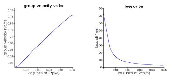
These results look reasonable, as we expect this loss to increase closer to the band-edge as the group velocity decreases.
Related publications
K. Ogawa et al., "Broadband Variable Chromatic Dispersion in Photonic-Band Electro-Optic Waveguide", OThE4, OFC (2006)