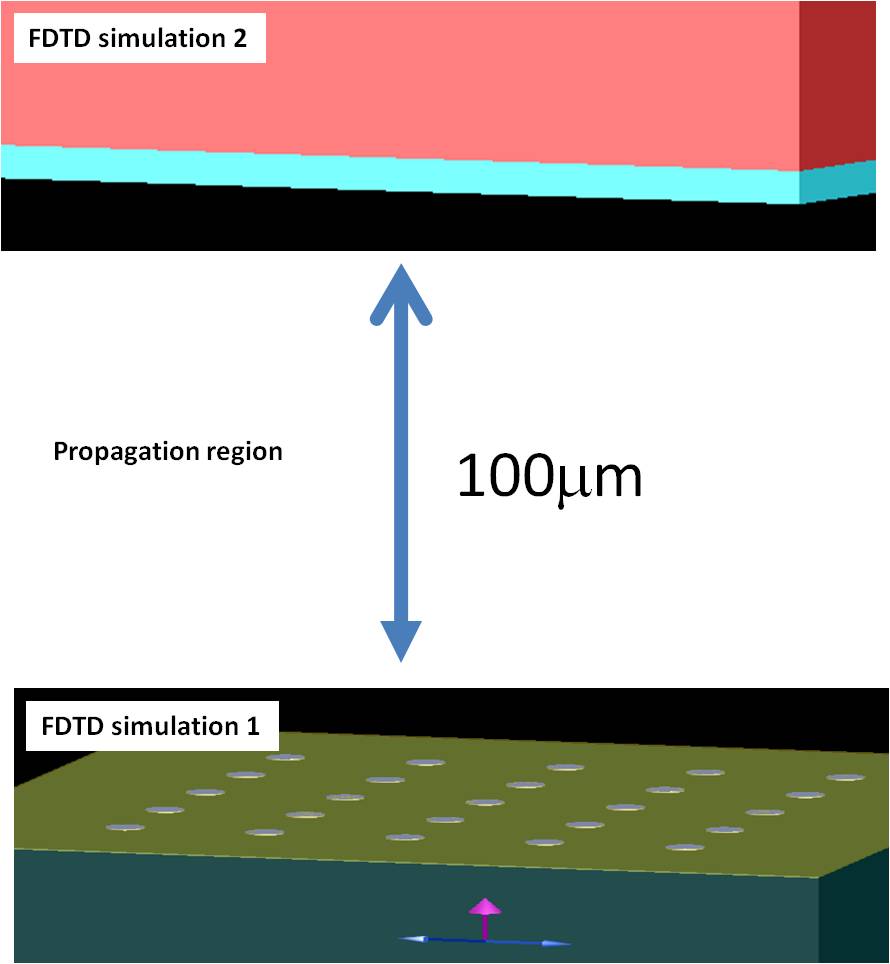
In this example, we will project the fields from the a periodic structure to a distance of 100 microns and then use the resulting fields to create a new FDTD source to study the electric field intensity in a layer of photoresist on silicon. This involves 3 steps:
1. FDTD simulation 1 where we simulate the periodic structure
2. Field projection stage where we propagate the fields 100 microns and create an mat file
3. FDTD simulation 2 where we create a source from the mat file and simulate the light as it enters the photoresist layer.
Step 1: FDTD simulation 1
The example file propagate_periodic1.fsp shows a thin film of gold on glass which has a circular etch hole in it. The simulation volume represents one unit cell of a periodic structure which has a period of 1.5 microns in both the x and y directions. The source covers a wavelength range of 0.4 to 0.6 microns, and is polarized with the E field along the x-axis. We take advantage of the symmetry of the structure to reduce the simulation volume to 1/4 of the unit cell. This is the same structure as shown in the previous section, but now we simulate only a small z-span of the structure because we can propagate the light using the plane wave decomposition method. In addition, we have a mesh override region to force a 10nm mesh around the hole for more accurate results. Please note that this simulation file can record the fields at many different wavelengths from 0.4 to 0.6 microns. In this case, we have recorded information at 3 wavelengths. Please run this fsp file.
Step 2: Propagate the fields and create new source
Once the simulation is complete, we can run the script file propagate_periodic.lsf is used to project the field to a distance of 100 microns from the periodic structure surface. To do this, we set the variable z_project to 99.83 microns because the monitor recording the fields is 70nm above the surface of the structure, and the source we eventually use will be 100nm below the surface of the photoresist.
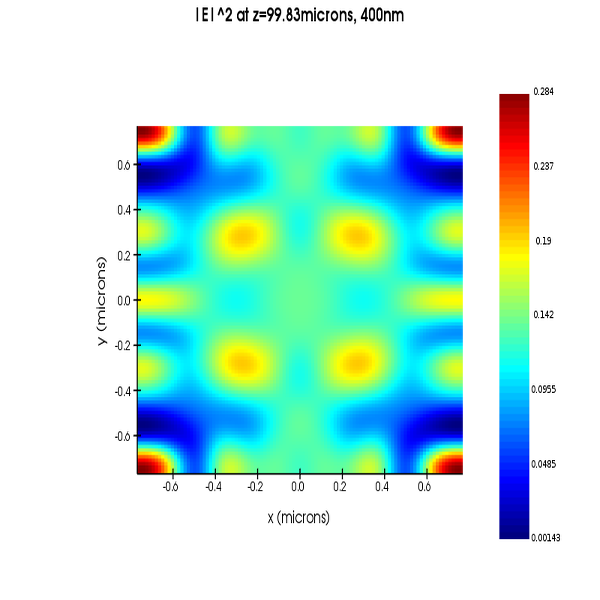
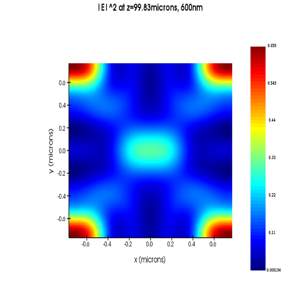
The projection is done for 3 recorded wavelengths. The field intensity pattern is very different at different wavelengths. After projecting the fields, a new mat file will be created that can be used to import the source into the second FDTD simulation. The default name for this file is EM.mat.
The fields 100nm below the surface of the photoresist are shown below:

Step 3: FDTD simulation 2
Open the simulation file propagate_periodic2.fsp. This file contains a simple 1 micron thick layer of photoresist on Silicon. For simplicity, we use an index of 1.7 for the photoresist and assume that it has no loss. Of course, more realistic material models can easily be created. This simulation file also uses a mesh override region to force dz of 10nm in the resist. This is useful to obtain a higher resolution on the field distribution in the resist.
Edit the source in this simulation region, and press the "Import Source" button. Browse to the mat file that was saved in the previous step and import the source. You can verify that the source field matches what was created in the previous step by pressing the "Visualize Data button" in the Edit Import Source window.
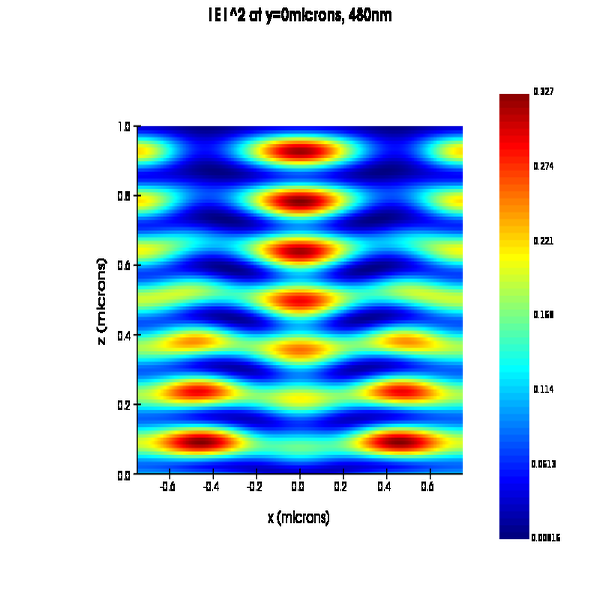
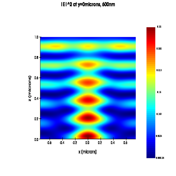
Run this simulation. It contains a monitor called volume_monitor that records the 3D field intensity inside the photoresist. The simulation is run for 3 recorded wavelengths.
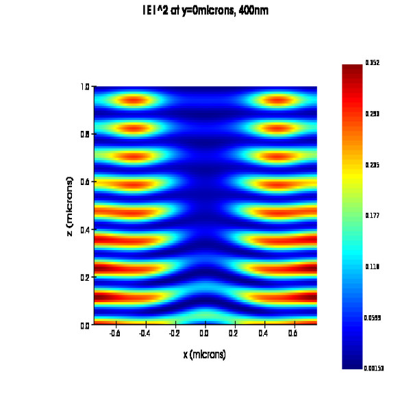
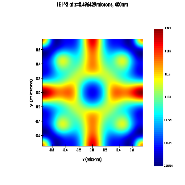
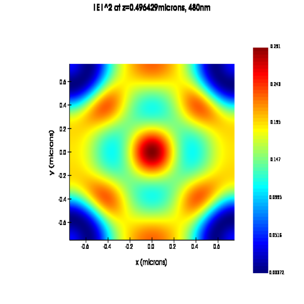
Results
Using the Visualizer, you can easily image different cross sections of the monitor called volume_monitor. For example, a cross section of |E|2 in the x-z plane at y=0 is shown below.
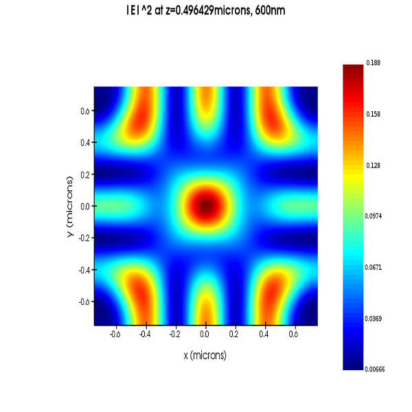
Similarly, a cross section of |E|2 in the x-y plane at z=0.5 microns depth is shown below.
See also
Solvers - Far field projections from periodic structures
Simplified Microscopic Imaging