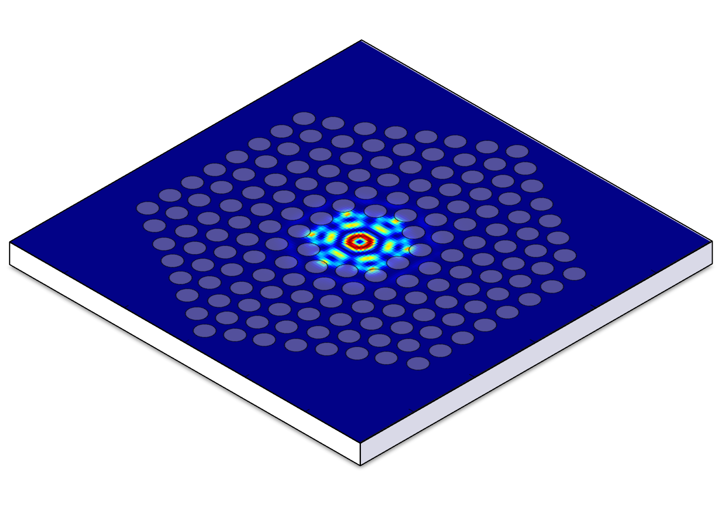
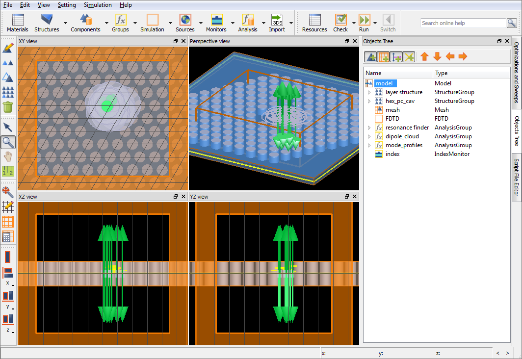
The goal of this example is to demonstrate how FDTD may be used to analyze photonic crystal nanocavities such as the one shown below. This is accomplished by reproducing the results in the paper by Y. Tang. This paper contains detailed information on the cavity structure as well as experimental and simulated data to compare against.
Using the techniques described in this example, it is possible to study other PC cavities. Since FDTD can simulate arbitrary geometries and materials, it is possible to adapt the methods presented here to study any micro/nanoscale cavity.
Summary of results
Using FDTD, we can calculate the resonant spectra of the cavity created by removing the center hole (H1) or by removing the center hole and the next ring of holes (H2).
For the H1 cavity, we compare using a constant dielectric model with a physically realistic GaAs/AlGaAs material model, as shown below. The peak spectra correspond well with the published results.
For H2 cavity, we can look at the spectrum to identify the 8 resonances found in the paper. Then use symmetry and anti-symmetric boundaries to isolate degenerate modes.
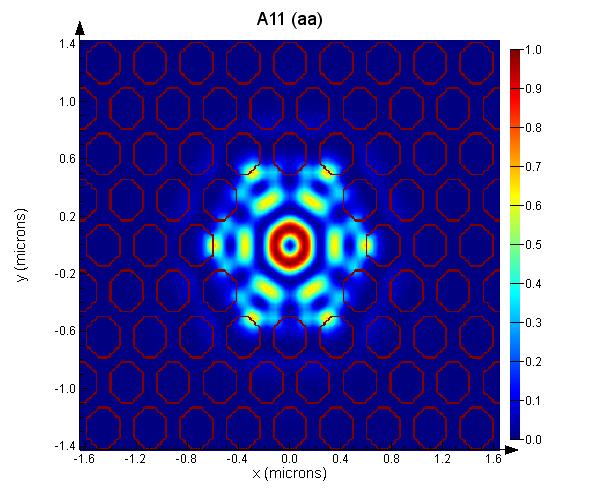
Finally, we show how to calculate and plot all the modes of the H2 cavity. For example, the A11 mode is shown below.
Simulation setup
Structure overview
The structure is formed on a thin GaAs / AlGaAs membrane suspended in air. For the purposes of this analysis, layer structure is assumed to be 170nm of GaAs sandwiched between 45nm layers of AlxGa1-xAs with x=0.3. Note that in the publication, the layers are 40nm of AlGaAs and an additional 5nm layers of GaAs, however, the 5nm layers are not expected to modify the results substantially, and yet would required a finer mesh size. For this reason, we have simply made the AlGaAs layers 45nm thick instead of 40nm. The total layer thickness is 260nm. This layer structure is contained in a structure group. This group allows you to use a constant dielectric for all the layers with a value of n=3.4 (the same as the value used in the simulations of the publication) or, alternatively, to use experimental data for GaAs from Palik, and a theoretical model for AlxGa1-xAs with x=0.3.
The theoretical model is generated by the script AlGaAs_Adachi.lsf, which saves a text file of values of n and k, which was then imported into the material database as a new material.
The photonic crystal consists of a triangular lattice of air holes in the membrane. The pitch of the lattice, a, is 366nm. For this example we will consider the case where the radius of the holes is 0.37a = 135.4nm.

The cavity is created using one of the structures from the Components Library. This structure is fully parameterized and allows the user to select the various parameters such as the pitch, H_number, etc. The material for the holes is set to etch. The layer structure is compose of 3 rectangles, which are grouped and parameterized as described previously. Finally, key parameters have been added to the model, as shown below. These parameters are set by the model and will override any direct settings of the children.
The cavity is created by removing either the center hole (H1) or the center hole plus the next ring (H2). This can be achieved by setting the H_number in the model to 1 or 2. The H1 cavity is shown below.
Controlling the mesh
For periodic structures it is best to make the mesh size periodic with the structure since this yields the best accuracy for a given mesh size. Setting a small mesh size will increase the calculation time and increase the accuracy of the result. The approach used here is to start with a coarse mesh to obtain initial results and understand the physics of the problem and then, if desired, to move to a fine mesh to obtain the final answer. We control the mesh in the x and y directions by adding a mesh override region and directly setting the value of dx and dy. For the z direction, we can allow the auto non-uniform meshing to choose an appropriate mesh. Initially, we can set the mesh accuracy slider of the simulation region to 2, which will control the z mesh. For the x and y meshes, we can choose a coarse mesh with 10 points per period of the PC (36.6nm grid). Since we are using a triangular lattice, we set the y mesh cell size to be sqrt(3)/2 times the x grid cell size. This ensures that the FDTD mesh is perfectly periodic in the y direction and yields better accuracy for a given mesh cell size. This setup is handled by the model so it is sufficient to choose the "grid points per pitch" property and set it to 10. The model then sets the corresponding values of dx and dy for you.
The simulation region
The second task is to set the size of the simulation area. The larger the simulation area, the longer the calculation will take, so we want to choose the smallest area that provides an accurate result. For the lateral dimensions of the FDTD area, we need to include enough rows of PC lattice to produce a bandgap. Since this is a high index contrast PC, 3 or 4 rows of holes surrounding the cavity is a good place to start. An X span of 3200nm and a Y span of 3200*sqrt(3)/2 will encompass 3 to 4 rows of PC holes. In the vertical dimension, we need to include some air above and below the slab since there is an evanescent field that decays into the air. We will start by including ~500nm of air above and below the slab. Once an initial result has been obtained, we can conduct an error analysis to verify that the simulation dimensions are sufficiently large. Note that the model will also enforce that the x span and y span's are integer multiples of the pitch (or sqrt(3)/2 times the pitch in the case of the y span) - you may notice that if you set the x span to 3200nm, when you re-edit the object it has been adjusted to 3294nm which is 9 times the pitch of 366nm. This, along with the settings in the mesh override region, will ensure that the FDTD mesh is identical for each period of the structure. This is important for measuring quality factors (Q) correctly for periodic devices.
Set the simulation time to 2000 fs. The simulation time length will be discussed in the source properties section.
The boundary conditions used for simulating a finite sized object such as the PC cavity are known as the PML (Perfectly Matched Layer). These boundary conditions absorb incident radiation. The PML boundary condition is the default when a new simulation area is created. There are 2 key changes that need to be made to the default PML settings, and these can be done in the Advanced Options of the FDTD Simulation region:
- Uncheck the " extend structure through pml" checkbox. For photonic crystals, we can actually get better PML performance if we allow the PC to extend into the PML. Without this, the last layer of materials at the edge of the boundary will be automatically extended completely through the PML.
- Set the value of "pml kappa" to 5. The pml, in combination with the dispersive materials that we will be using, can lead to increased numerical instability in the PML. This can be controlled for reasonable simulation times by increasing the value of PML Kappa.
It is also possible to employ symmetry boundary conditions in cases where the structure itself exhibits symmetry. Symmetry boundary conditions can reduce computation time, however, the cost is that they will forbid certain modes from appearing in the results (modes that do not exhibit the same symmetry relation as the boundary condition). For this PC cavity, there is a plane of symmetry through the center of the slab (z=0 plane). Using a symmetric boundary condition on this plane will only allow TE modes and eliminate TM modes from the results. Since this structure has little or no TM bandgap and the cavity modes are expected to be TE, we will use the symmetric boundary condition on this boundary.
Finally, when studying resonators, it is a good idea to disable to the autoshutoff feature of FDTD. This is because a high Q resonator, which traps light over a very small bandwidth, may only trap a small fraction of the original excitation energy which is broadband. As a result the autoshutoff can trigger too early and cause problems with our time apodization of monitors. The autoshutoff can be disabled by unchecking the "use early shutoff" in the Advanced Options tab of the FDTD simulation region.
Source pulses and simulation time
To excite the cavity, we add some dipole sources. These sources are added by an Analysis Group which creates a random set of dipoles over a given area. The area is controlled by the model and is based on the chosen H number (for larger cavities, the cloud of dipoles is extended). Also, these dipoles are added in the upper right quadrant only, in anticipation of simulations with symmetric and anti-symmetric boundary conditions. These sources will inject a short pulse of radiation to excite a broad range of frequencies. In order to effectively excite the cavity modes we need to ensure that the polarization of the dipole sources is similar to the polarization of the modes we wish to excite. In this case we want to excite TE modes so we will use a vertically (z) polarized magnetic dipole. We also need to ensure that the dipole sources are placed in locations where the mode profiles do not exhibit nulls. To accomplish this we use a random set of dipoles over the desired area. If we wanted to excite TM modes we would use vertically polarized electric dipoles, and we would have to change or z min boundary condition to Anti-Symmetric.
The final step in setting the sources is defining the excitation pulse. This is done by simply selecting the appropriate wavelength range that we want to study. In this case, we choose 1000nm to 1400nm. We used the global source properties to do this, to avoid having to make the changes for each dipole individually. Note that each dipole must be set to use the global source properties, which is not the default.
The simulation time defined in the simulation region properties is 2000fs and much longer than the pulse length. This is because we want to monitor the fields in the cavity after the pulse has excited modes. Analyzing the fields in the cavity after the initial pulse will reveal the frequencies of the cavity modes.
Simulation monitors
There is an analysis group of monitors called "resonance finder". Fourier transform analysis of these time signals will reveal the cavity mode frequencies. This is handled automatically by the analysis script in the group. By default, we choose to use 8 total time monitors which are spread randomly over a region of the cavity. The extent of these monitors is set by the model and depends on the H_number chosen for the cavity. This helps us avoid any nulls of particular modes.
There are also frequency domain profile monitors to capture the modal fields. These monitors are stored in an analysis group called mode_profiles. This analysis group can find the mode profiles of up to 12 modes. The user must specify the resonant frequency of the modes and the desired apodization settings. The apodization settings are critical to finding the right mode profile. For more details on apodization settings, please see the Apodization in the User Guide under Monitors and Analysis Groups.
Results - H1 cavity
The H1 cavity is formed by removing a single hole from the photonic crystal, as shown in the figure below. This can be accomplished by setting the H_number property to 1 in the model.

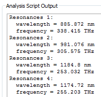
Load and run the simulation file Tang_cavity.fsp. Then edit the "resonance finder" object and press the "Run Analysis" button which will generate the following figures and results.
Plotting the spectrum as a function of normalized units of (a/lambda) is also possible with the script commands below, which can be pasted into the script prompt, or used to create a new script file:
select("::model");
a = get("a");
mname = "resonance finder";
runanalysis(mname);
f = getdata(mname,"f");
spectrum = getdata(mname,"spectrum");
plot(f*a/c,log10(spectrum),"frequency (a/lambda)","spectrum (a.u., log scale)");
setplot("x min",0.2);
setplot("x max",0.44);
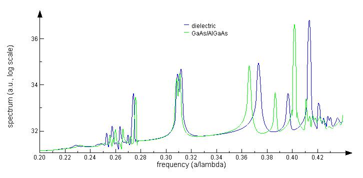
This will generate the following figure
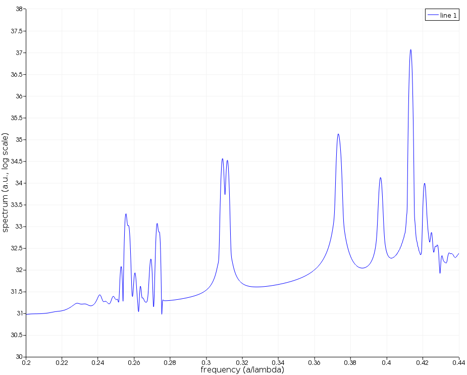
In this example there are a number of peaks present in the result. These peaks correspond to cavity modes and bandgap edges. Often peaks are observed at the bandgap edges since the modes at these frequencies have a very low group velocity and do not decay away very quickly. The 2 peaks that correspond to the cavity modes appear at approximately 0.31 and 0.37, in reasonable agreement with the results for the first and second order modes in the Y. Tang paper, which were also calculated assuming a constant permittivity for the slab.
Note that we can rerun the simulation with using a GaAs and AlGaAs model for the materials. This can be accomplished by setting the property "use constant dielectric" of the "layer structure" group to 0. The figure below compares the results.
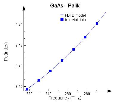
We can see that the spectra agree well at lower frequencies but there is a shift at higher frequencies. This shift makes sense when we consider that the GaAs makes up 170nm of the 260nm layer and has in index higher than 3.4 at higher frequencies, as shown below.
In the remainder of the example, we will use a constant dielectric model. This should give the best agreement with the simulated results of Tang et al., however the dispersive model should give better agreement with the experimental results.
Next steps
- To resolve the mode profiles of the cavity modes we can adjust the frequency domain profile monitor settings (center frequency and apodization) to calculate the mode profiles of these resonances.
- To learn more about the symmetries of the modes and look at mode profiles of degenerate modes, we can apply various combinations of symmetric and anti-symmetric boundary conditions to the x=0 and y=0 planes and repeat the simulation.
- To gain a highly accurate result, we can repeat the simulation with a finer grid size. It may also be useful to investigate any effects of moving the PML boundaries further from/closer to the cavity.
We will demonstrate most of these steps in the next section when we look for H2 cavity modes.
Results - H2 cavity
To study the H2 we simply need to change the H_number in the model to 2.
First results
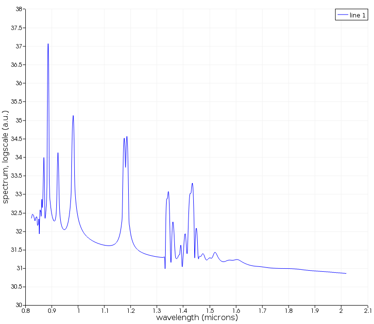
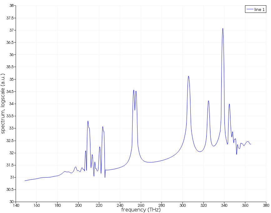
After running the simulation, the following script can be used to plot the spectrum in normalized frequency units of (a/lambda):
select("::model");
a = get("a");
mname = "resonance finder";
runanalysis(mname);
f = getdata(mname,"f");
spectrum = getdata(mname,"spectrum");
plot(f*a/c,log10(spectrum),"frequency (a/lambda)","spectrum (a.u., log scale)");
setplot("x min",0.27);
setplot("x max",0.36);

Looking at these results we can immediately see that there are 8 peaks in the frequency range of interest (we have restricted to looking at the approximate frequency range where experimental results exist). The frequencies of the peaks are within a few percent of the experimental results, although it is not immediately obvious which peak in the simulated results necessarily matches up with each experimental peak. We also have an extra peak in the simulated results that is not identified in the experimental data. In general the agreement is quite good for a first attempt.
We can also see that two of the peaks appear to be split - this is likely because these correspond to theoretically degenerate peaks where the degeneracy is broken by the cartesian simulation mesh. On a triangular lattice, modes can be degenerate based on a 60 degree lattice symmetry. The cartesian mesh can artificially break this symmetry, and this effect will be more apparent on a coarse mesh. We can rerun the simulation on a finer mesh by
- Setting the "grid points per pitch" property of the model to 20 instead of 10. This will halve the size of dx and dy.
- Increasing the mesh accuracy slider of the FDTD simulation region to 4 instead of 2.
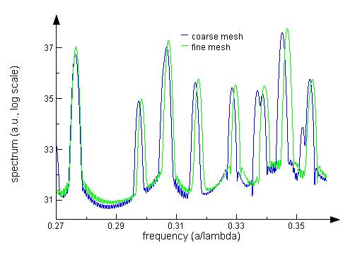
If we rerun the simulation (which now takes significantly longer), we can compare the results on a fine and a coarse mesh, shown below. We see that there is reasonable agreement between the 2 results, with a frequency shift that generally becomes larger at higher frequency (shorter wavelength), which is expected. We also see that the splitting of the peaks disappears with a finer mesh. However, the coarse mesh is surprisingly accurate, especially when considering that, at a wavelength of 1000nm, lambda0/(n*dx) ~ 8. This is partly a consequence of using Lumerical's conformal mesh technology which makes it possible to obtain good results at coarser mesh sizes. For the remainder of this example, we will continue to work at a coarse mesh. For publication quality results, we should repeat several more simulations to ensure that the results have converged to within our tolerances.
Detailed analysis
To understand the problem further, we are going to use symmetry and anti-symmetry to classify the modes. We are also going to use our frequency domain profile monitors to calculate the mode profiles. The first step is to add the frequency domain power monitors and adjust their frequency and apodization settings.
- Apodization. The simulation runs for 2000fs. We should choose full apodization, a time center of 1000fs, and a time width of 200fs. This means that the FHWM of the apodization spectrum will be 4*log(2)/(2*pi*200fs) ~ 2 THz. Choosing this apodization means that peaks should be separated by more than 2THz, and that we will measure the correct mode profile as long as we choose a frequency for our monitor within about 2THz of the correct peak. Plotting the spectrum in un-normalized units, we can see that this should not be a problem. For more details on apodization, please see the Apodization in the User Guide under Monitors and Analysis Groups.

- Frequency settings. We want to add 8 monitors with frequencies between 220 and 300 THz. In reality, we will add 9 monitors to account for the artificial double peak at 276 THz.
These monitors can be added by hand, but the simulation contains an analysis group called mode_profiles that is designed to add up to 12 frequency monitors in the x-y plane. This makes it easy to adjust the apodization settings for all monitors. To simplify calculating the 9 resonant frequencies, the script file Tang_cavity_setup_profile_monitors.lsf will calculate the 9 resonances within the desired bandwidth and set the frequencies of the mode_profile analysis group accordingly. The resonant frequencies must be reset any time there are changes to the mesh accuracy, material settings or any other settings that could cause the resonant peaks to shift.
Mode Symmetry
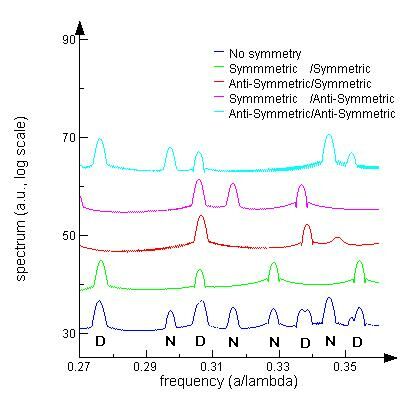
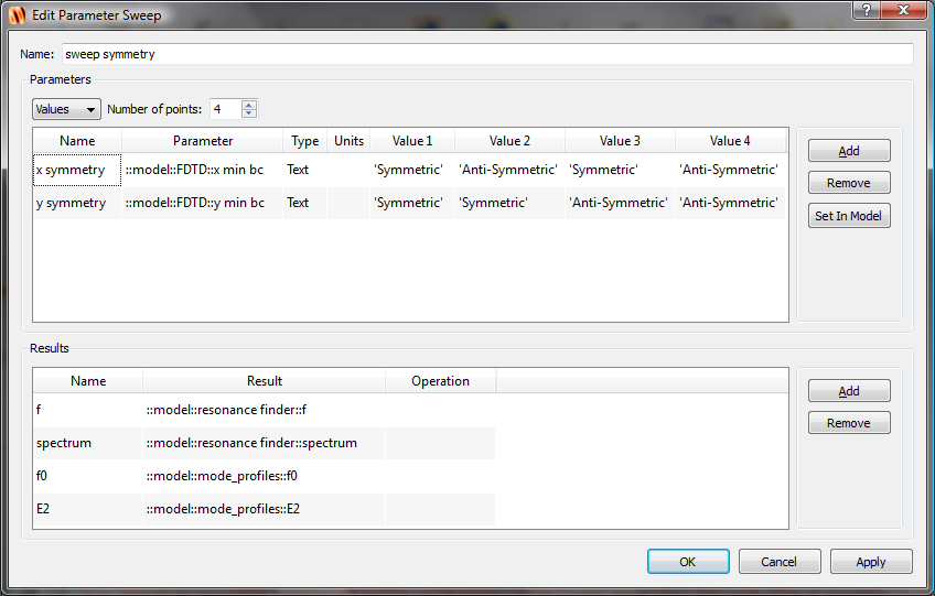
The next step is to consider the symmetry of the modes. We will do so by repeating the simulation 4 times using the different combinations of symmetric and anti-symmetric boundary conditions on the x=0 and y=0 planes of symmetry. Each of these simulations take ~1/4 of the time to run as the full simulation. This can be accomplished using the "sweep symmetry" object included with this example. This object can be found in the Optimization and Sweeps window.
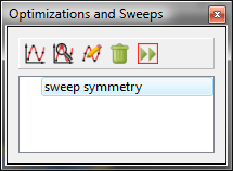
Editing the object shows that it is configured to run 4 parameter sweeps, and each time it will apply a different symmetry condition to the min x and min y boundaries.
After running the parameter sweep object, the following lines of script will plot all the spectra. These lines are also saved in the file Tang_cavity_symmetry.lsf.
select("::model");
a = get("a");
mname = "resonance finder";
runanalysis(mname);
f = getdata(mname,"f");
spectrum = getdata(mname,"spectrum");
sweepname = "sweep symmetry";
spectrum_sym = pinch(getsweepdata(sweepname,"spectrum"));
plot(f*a/c,log10(spectrum),
           log10(pinch(spectrum_sym,2,1))+8,
           log10(pinch(spectrum_sym,2,2))+16,
           log10(pinch(spectrum_sym,2,3))+24,
           log10(pinch(spectrum_sym,2,4))+32,
           "frequency (a/lambda)","spectrum (a.u., log scale)");
legend("No symmetry",
       "Symmmetric    /Symmetric",
       "Anti-Symmetric/Symmetric",
       "Symmmetric    /Anti-Symmetric",
       "Anti-Symmetric/Anti-Symmetric");
setplot("x min",0.27);
setplot("x max",0.36);
The figure below shows the resulting plot. The legend indicates if no symmetry was used, or when symmetry was used at the x min/y min boundary. For example Symmetric/Anti-Symmetric means that the x min boundary condition was Symmetric, while y min was Anti-Symmetric. In general the results show that certain peaks are present with only one combination of symmetry boundaries (non-degenerate mode) while other peaks show up for multiple combinations of symmetry boundaries (degenerate modes). Each peak in the data figure below is marked with either a "D"or a "N" to indicate a degenerate or non-degenerate mode.

We can now refer back to the experimental results presented in the Y. Tang paper and identify the simulated modes with the experimental modes. The following table lists the mode frequencies from the Y. Tang paper along with their degeneracy as determined by the line width/polarization analysis. It is now easy to see which modes in the simulated data correspond to the experimental data. The results are summarized in the table below.
|
Peak # (Mode) |
Degeneracy |
Experimental freq. |
Simulated freq. |
|
1 (E11) 2 (A11) 3 (E12. E13) 4 (B2) |
D N D N |
0.285 0.306 0.312 / 0.313 0.323 |
0.276 0.297 0.307 0.316 |
|
5 (A2) |
N |
0.329 |
0.328 |
|
6 (E14) 7 (A12) |
D N |
0.341 0.348 |
0.337/0.339 0.345 |
|
8 |
D |
NA |
0.354 |
The results in the preceding table show that the 8th peak in the simulated data was a degenerate mode that was slightly higher in frequency than the quantum dots could excite in the experiment. Knowing that this mode is there, you can actually see a very small bump in the experimental data around 0.352 that might correspond to this mode.
The simulation data is in very good agreement with the experiment. The worst case difference in model versus experiment is ~3.5%, which is consistent with the worst case difference in the plane wave model (as compared to experiment). The average difference in experimental versus simulated mode frequencies is less than 2%. This is quite good agreement for the simple model that we have used. The results could certainly be improved by using a finer mesh, using more realistic material models, and making sure that the simulated structure dimensions is in agreement with the experimentally fabricated device, for example, by defining the structure using an SEM import.
Results - H2 cavity mode profiles
In the previous step we ran a number of simulations with different symmetry settings. We also configured the mode_profiles analysis group object to have a monitor recording the electric field at each of the 9 resonant frequencies, with appropriate time apodization settings.
In addition to collecting the spectrum for each symmetry setting, the parameter sweep object also collected a matrix of |E|2. In each simulation, this matrix is created by the mode_profiles analysis group. The parameter sweeps collates all of this data into a single matrix. At the end of the sweep, we have a variable called E2 which is a 4D matrix, of size length(x) X length(y) X 9 X 4. The first 2 dimensions are the x and y axes in the x-y plane. The third dimension corresponds to the 9 resonant frequencies collected, and the final dimension is the 4 values of parameter sweep that we ran, corresponding to the 4 possible symmetry/anti-symmetry combinations.
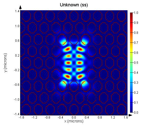
The script file plot_modes.lsf gets the 4D matrix E2. It then interpolates onto a finer mesh, and collects some structure outline results from the index monitor to create a higher resolution matrix for better imaging of the results. It then plots different results by choosing specific resonant frequencies, and specific symmetry/anit-symmetry conditions. Each figure is automatically exported to a jpg file. The results are shown below.
Degenerate modes
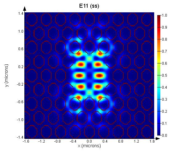
E11
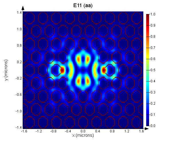
E11
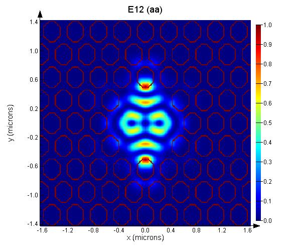
E12

E12

E13
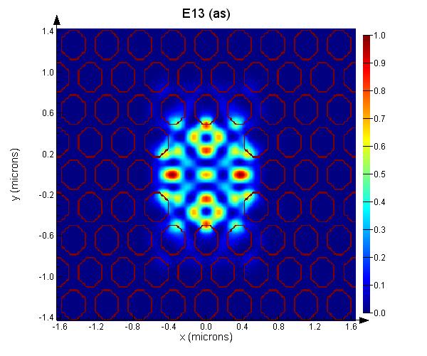
E13

E14
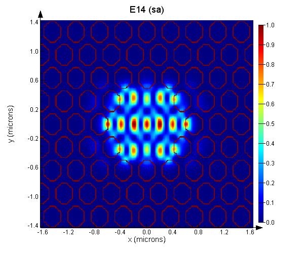
E14
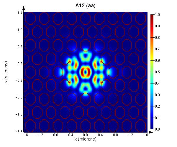
Non-degenerate modes
A11
A12

A2
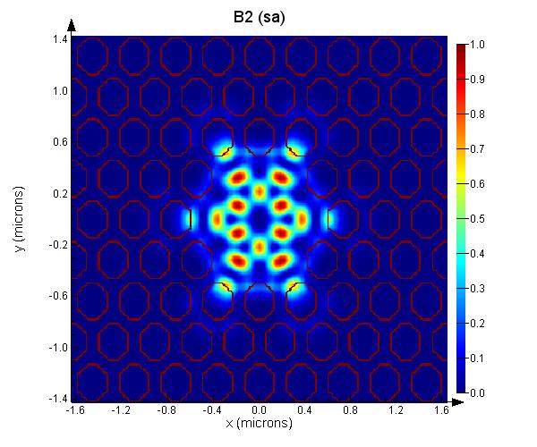
B2
The mode profiles presented here agree very well with those presented in the Y. Tang paper that were calculated using a plane wave model.
Using the varFDTD solver
The goal of this section is to demonstrate how the varFDTD solver in MODE may be used to analyze photonic crystal nanocavities such as the one shown below. This is accomplished by reproducing the results in the paper by Y. Tang. This paper contains detailed information on the cavity structure as well as experimental and simulated data to compare against.
Setup
The completed simulation file,[[cavities_3Dpcm.lms]], can be downloaded from the "Associated files." See the FDTD example for an in depth discussion on the optimal way to setup the simulation. Overall, the setup of this simulation in MODE is very similar to FDTD. The structures can be copied directly from the FDTD example file. The simulation region, sources and monitors should be setup in a similar way. Of course, while the setup is very similar, a few differences exist:
- Propagator object - Effective index tab: We will use the default settings, including the Narrowband option, which will neglect any slab dispersion. For improved accuracy, you can try using the Broadband option.
Results
The simulation is very quick and should be finished in a few seconds. Next, run the Qanalysis object to find the resonant frequencies. This involves a large number of fft's and will take a couple of minutes. The following commands can be used to output the results to the script prompt. The Qanalysis object can also be used to plot the spectrum (and filters used for the calculation).
runanalysis;
Q = getresult("Qanalysis","Q");
?Q.f/1e12;
?Q.Q;
result:
192.376
207.302
197.875
result:
202.889  293.017  237.532
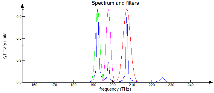
The amplitude of each resonance is not very meaningful, as it depends on the position of the sources used to excite the system and the position of the time monitors used to measure the response.
From the calculated resonant frequencies, we can set up two profile monitors in order to obtain their profiles and each monitor can monitor two frequencies. After re-running and averaging the 3 analysis groups, the results are summarized as below
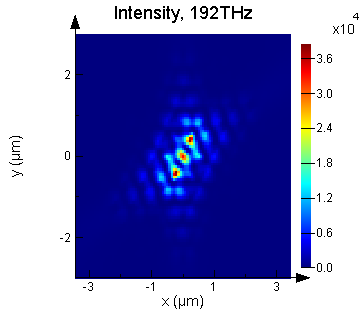
Frequency: 192.4 THz, Q: 198
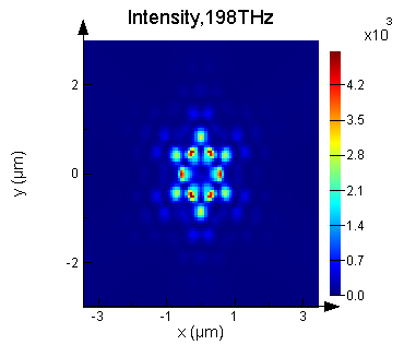
Frequency: 197.9 THz, Q: 293
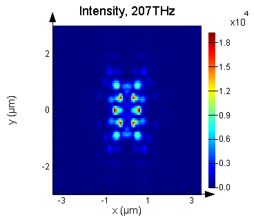
Frequency: 207.3 THz, Q: 239
Related publications
Tang, Y. Mintairov, A.M. Merz, J.L. Tokranov, V. Oktyabrsky, S., Characterization of 2D-photonic crystal nanocavities by polarization-dependent photoluminescence, 5th IEEE Conference on Nanotechnology, July 2005, vol. 1, pp 35-38