 This page describes a simple and easy to understand approach to calculate absorbed optical power per unit volume (Pabs) due to material absorption. Once Pabs is known, it is easy to calculate total absorption in some volume by integrating the loss function over that volume. A more numerically accurate version of the calculation is described in Advanced method. Calculating the divergence of Poynting vector is an alternate approach to get Pabs.
Theory
The absorption per unit volume can be calculated from the divergence of the Poynting vector,
$$ P_{abs} = - 0.5 \ real(\nabla \cdot P) $$
It is possible to calculate the absorption directly from this formula (see the Divergence of Poynting vector section), but divergence calculations tend to be very sensitive to numerical problems. Fortunately, there is a more numerically stable form. It can be shown that the above formula is equivalent to
$$ P_{abs} = - 0.5 \ real(i \omega E \cdot D) $$
With a little more work, we get the desired result
$$ P_{abs} = -0.5 \ \omega \vert E \vert ^2\ imag(\varepsilon)$$
To calculate the absorption as a function of space and frequency, we only need to know the electric field intensity and the imaginary part of the permittivity. Both quantities are easy to measure in an FDTD simulation.
Simulation setup
The example simulation is composed of an Air - Glass - Si stack. A focused beam is incident on the stack. Air and Glass are not lossy materials, so we only expect absorption to occur in the Si layer.
A 3D power monitor is used to measure the electric field intensity. Similarly, an index monitor is used to measure the permittivity. Both monitors should be the same size. 3D monitors tend to require large amounts of memory, so they should be kept as small as possible. In this example, both monitors cover the entire simulation region, but this is only to demonstrate that the loss is zero in the Air and Glass regions.
The simulation setup is shown in the following figure.

|
Note: Check memory requirements Since 3D monitors require large amounts of memory, be sure to use the Check memory requirements button before running the simulation. In this example, about 100MB of data is collected. Up to 1GB is required to run the analysis script. Memory requirements for larger simulations can be much higher. |
|
Note: Reducing memory requirements If the memory requirements are too large, consider making some of the following modifications:
|
Calculating Pabs
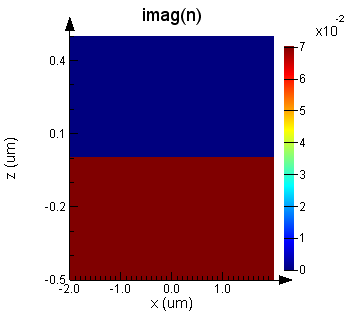
Run the simulation with FDTD mesh accuracy of 2 and then run the analysis script, which will create a number of figures. The first three figures show a cross section of the electric field intensity and material properties at y=0 for the second frequency point (at a wavelength of 500nm).
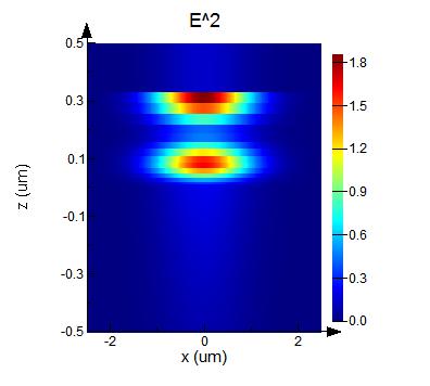 |
The electric field intensity. The figure can be divided into 4 regions.
|
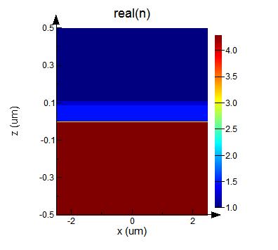 |
The real part of the refractive index. There are three materials in this simulation.
|
|
|
The imaginary part of the refractive index. The imaginary part is a measure of the material loss. Loss will only occur in materials with k>0.
|
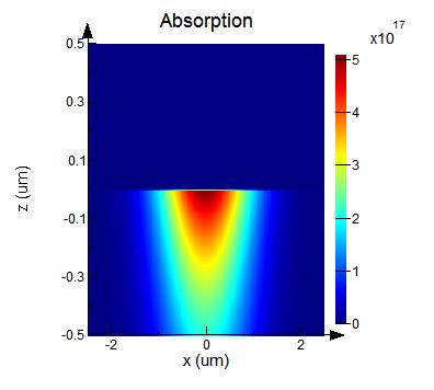
From this data, the script calculates the material absorption as a function of space and frequency. A cross section of the absorption function is shown below. Notice that loss only occurs in the Si layer.
Total absorbed power
The total absorbed power can be calculated in two ways:
- Integrate the loss function over the entire simulation volume.
- Use the transmission function and a set of 2D power monitors to measure the amount of power flowing into and out of the Si layer. The difference between these values will be the material absorption. In this example, T2 measures the power flowing into the Si, and T1 measures the power flowing out. To be strictly correct, there should also be monitors at the sides of the Si layer, but they were not added to this simulation because most of the power is flowing in the Z direction.
Both techniques give similar results. If a smaller mesh size was used (default mesh accuracy=2), the results would be even closer. Also, although we don't see it in this example, the discrepancy can increase slightly at the shorter wavelength where the absorption of the Si is higher. This is due to some numerical errors in integrating the loss in the first dz of the Si and can be improved by using the Advanced method.
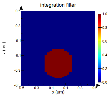
Absorbed power in spherical region
When calculating absorption within a rectangular region, a box of 2D power monitors is computationally more efficient (since it only requires surface data rather than volume data, and because the index monitor is not required). The primary reason for calculating the loss as a function of space is to integrate over non-rectangular regions. For example, imagine we want to calculate the total absorption within a spherical region. In such cases, we can calculate the loss as a function of space, then integrate over the spherical volume. It is also possible to define an integration filter using the material properties to define whether a point should be included or not included in the integration. See the Advanced method - multiple materials page for more information on how to do this.
The following figure shows a cross section of an integration filter for a sphere centered at (0,0,-200 nm) and a radius of 200nm.
The final output of the script is the percentage of power absorbed within the spherical region at a wavelength of 500nm: ~1%