Accurate bandstructure calculations are important for the design and analysis of photonic crystal devices. In this example, we will focus on how to use MODE' 2.5D FDTD propagation method to calculate the bandstructure of a slab photonic crystals device with a square and hexagonal lattice of holes.
For an introduction to calculating bandstructures using FDTD, see Rectangular Photonic Crystal Bandstructure.
Simulation Setup
In general, bandstructures can be calculated using a time domain method or using a plane wave expansion method. One advantage of using the finite-difference time-domain (FDTD) method is that one can calculate slab photonic crystals without band-folding effects. This technique is very useful for most photonic crystal devices compatible with CMOS technology, where the geometry is planar, with a non-periodic 3rd dimension. In this example, we use the 2.5D FDTD propagation method in MODE to calculate the bandstructure of a slab photonic crystal with a square and hexagonal lattice. We will also compare the results to that of 3D FDTD to show that the 2.5D FDTD method can give comparable results with a fraction of the memory and simulation time required by 3D FDTD.
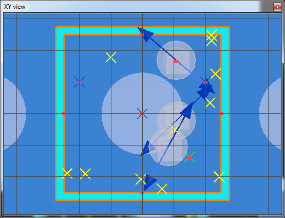
This example is similar to the Planar 3D example. Here, the membrane structure has thickness 200nm and a refractive index value of 3.4. A square lattice of holes with radius = 130nm have been etched into the layer, with the lattice period ax = 500 nm. Just like in the 3D FDTD example, the 2.5D FDTD "PROP" simulation region will cover exactly one period (unit cell) of the device. Note that the key parameters such as the period, start/stop frequencies are specified in the "model" analysis group, under Setup->Variables. The "dipole_cloud" analysis group contains randomly-distributed electrical dipoles used to excited the Bloch modes. The “bandstrucutre” analysis group contains randomly-distributed time monitors, and the time signals are combined and used to calculate the bandstructure. A sweep project “Gamma-X” has been created to sweep the k-vectors and locate the band gap for this square lattice. Note that this slab PC device supports TE and TM-like modes. By choosing “E mode(TE)” for the polarization option under the Effective index tab of the "PROP" simulation region, only the TE-like bandstructure will be calculated.
Since we are interested in the bandstructure over a large frequency range, it is important to verify the slab mode profile over the entire simulation frequency range. For example, if the start frequency is too small, the slab may not have a well-supported mode.
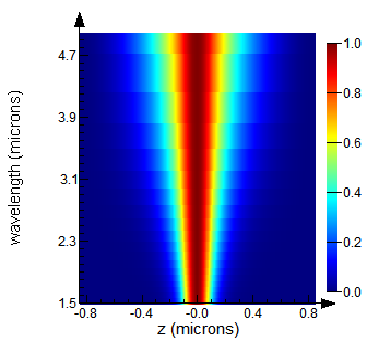
Correct, the slab mode is supported over the entire frequency range
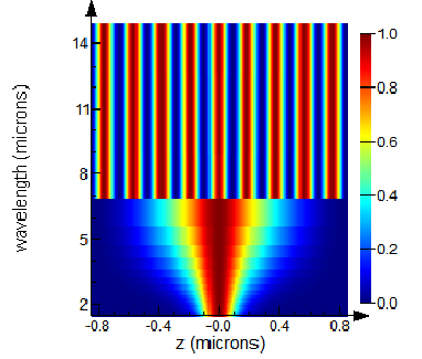
Incorrect, the slab is not supported at longer wavelengths.
Based on these considerations, we will choose the start/stop frequencies to be 60THz/200THz, which covers most of the first and the second bands.
Results and discussions
To begin, open planar_square.lms, and change the "bandwidth" option (under the Effective index tab of the "PROP" simulation region) to "broadband" (the "narrowband" option was used for the purpose of keeping the file sizes small, but the "broadband" option is necessary for accurate broadband results). Use the script file planar_square.lsf to run the Gamma-X parameter sweep and create the figures below. The left figure shows the bandstructure calculated using the 2.5D FDTD propagation method in MODE, and the right figure shows the same result using 3D FDTD.
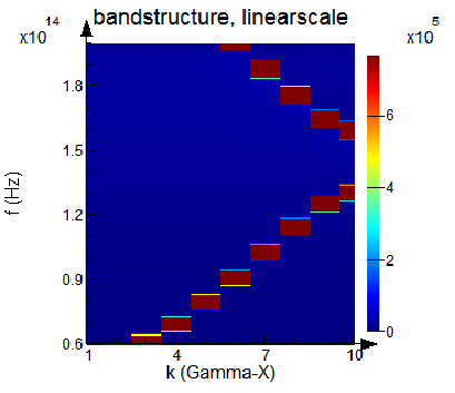
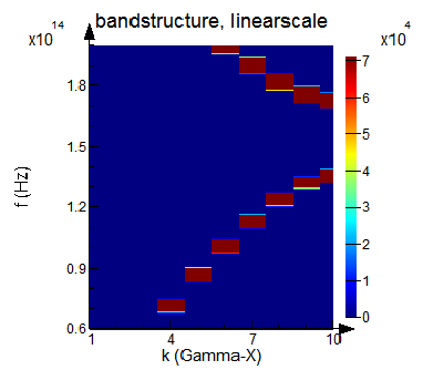
One can see that the results obtained using 2.5D FDTD and 3D FDTD are very similar.
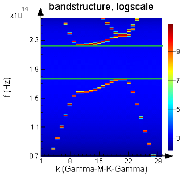
Hexagonal lattice
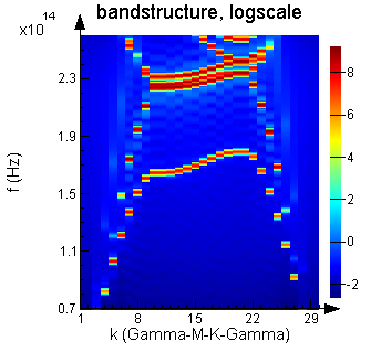
In this section, we will calculate the bandstructure for a hexagonal lattice similar to the one from the Photonic Crystal Waveguide example. To begin, open plannar_hex.lms, and change the "bandwidth" option (under the Effective index tab of the "PROP" simulation region) to "broadband". Use the script file planar_hex.lsf to run the Bloch wavevector parameter sweeps. The figures below show the bandstructure of the TE and TM-like modes. Note that there is no bandgap for the TM-like modes.
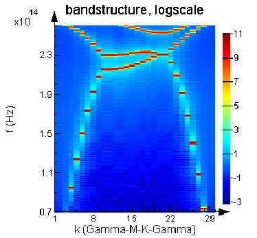
For comparison, the figure below shows the bandstructure calculated using 3D FDTD, including both the TE and TM-like modes. One can see that the agreement is very good, and we get a similar band gap between the two methods.
Calculating the bandstructure of a perfect photonic crystal is a good starting point for designing a photonic crystal waveguide. The fact that we can get comparable results between 2.5D FDTD and 3D FDTD means that we can use the 2.5D FDTD method to study slab photonic crystals devices efficiently. Depending on the type of defect and modification on the photonic crystal geometry surrounding the waveguide, the low transmission band will often not coincide with the band gap calculated for the perfect photonic crystal. In this case, the 2.5D FDTD method can be very useful for studying how the propagation of light in the photonic crystal waveguide is affected by modifications in the PC geometry.